Integrated semiconductor solar cell package

a solar cell and integrated technology, applied in the field of semiconductor photovoltaic device packaging, can solve the problems of high mechanical failure rate in actual use, photovoltaic device, current solar cell package design, etc., and achieve the effect of reducing the vertical profile of the device, facilitating hermetically sealing, and reducing the vertical and narrow horizontal profiles

Active Publication Date: 2012-08-09
CACTUS MATERIALS INC
View PDF5 Cites 12 Cited by
  • Summary
  • Abstract
  • Description
  • Claims
  • Application Information

AI Technical Summary

Benefits of technology

[0007]According to the invention, a device containing a solar cell is provided in the form of a stacked package that has a planar arrangement of conductive laminates at or below the surface of a heat sink. The planar alignment allows placement of electrical connections below the surface of the heat sink and reduces the vertical profile of the device, making it easier to be hermetically sealed. In specific embodiments the solar cell substrate is embedded within the heat sink during the manufacturing phase, eliminating the need for a thermally conductive substrate between the solar cell and the heat sink. The durable and easily manufactured solar chip packages have lower vertical and narrower horizontal profiles than heretofore, presenting a more versatile package and a less expensive manufacturing alternative to current chip packaging technologies. Electrical connections are made between the chip and protective bypass diodes or other external circuitry without the need for complex, time consuming, expensive, and vulnerable plastic packaging and soldered interconnections.

Problems solved by technology

Photovoltaic devices present unique problems requiring specialized packaging to achieve desired levels of durability, mechanical integrity, electrical connectivity, maximum thermal transfer, and convenience of mounting.
The delicate semiconductor material used as the operative portion of a solar cell must be protected from excessive current by attaching, for example, an additional device such as a bypass diode in parallel with the anode and cathode of the device, an operation normally accomplished by soldering surface mount plastic packaged devices in a manner that may cause high rates of mechanical failure in actual usage.
Current solar cell package designs suffer from design and component limitations that restrict package usage.
Because of the limited number of suppliers, use of these ceramic substrates increases the cost of manufacturing the solar packaging.
Commercialized solar packages also require that the chip, thermally conductive substrates, and heat sink be stacked vertically, increasing the profile of the package and thereby making hermetic sealing of the solar package more difficult and expensive.
A further limitation of solar packaging designs in current use is a maximum platform size of 4.5 inches×4.5 inches.

Method used


Image

  • Integrated semiconductor solar cell package
  • Integrated semiconductor solar cell package
  • Integrated semiconductor solar cell package

Examples


embodiments

Embedded Substrate Embodiments

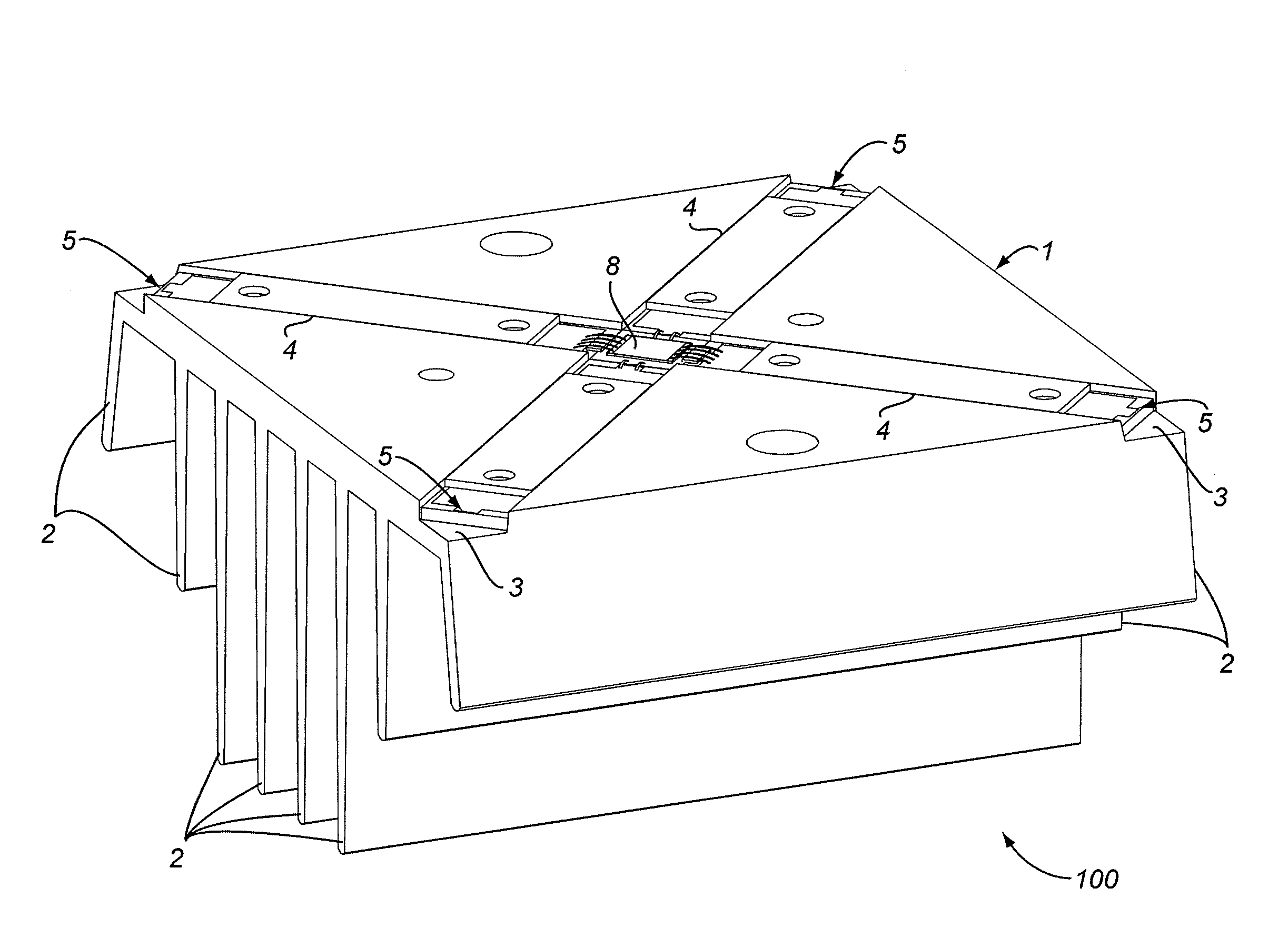
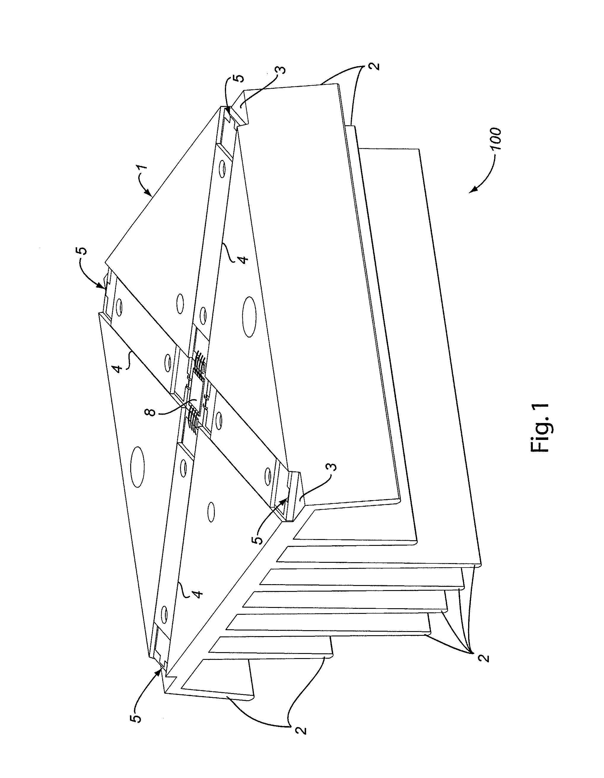
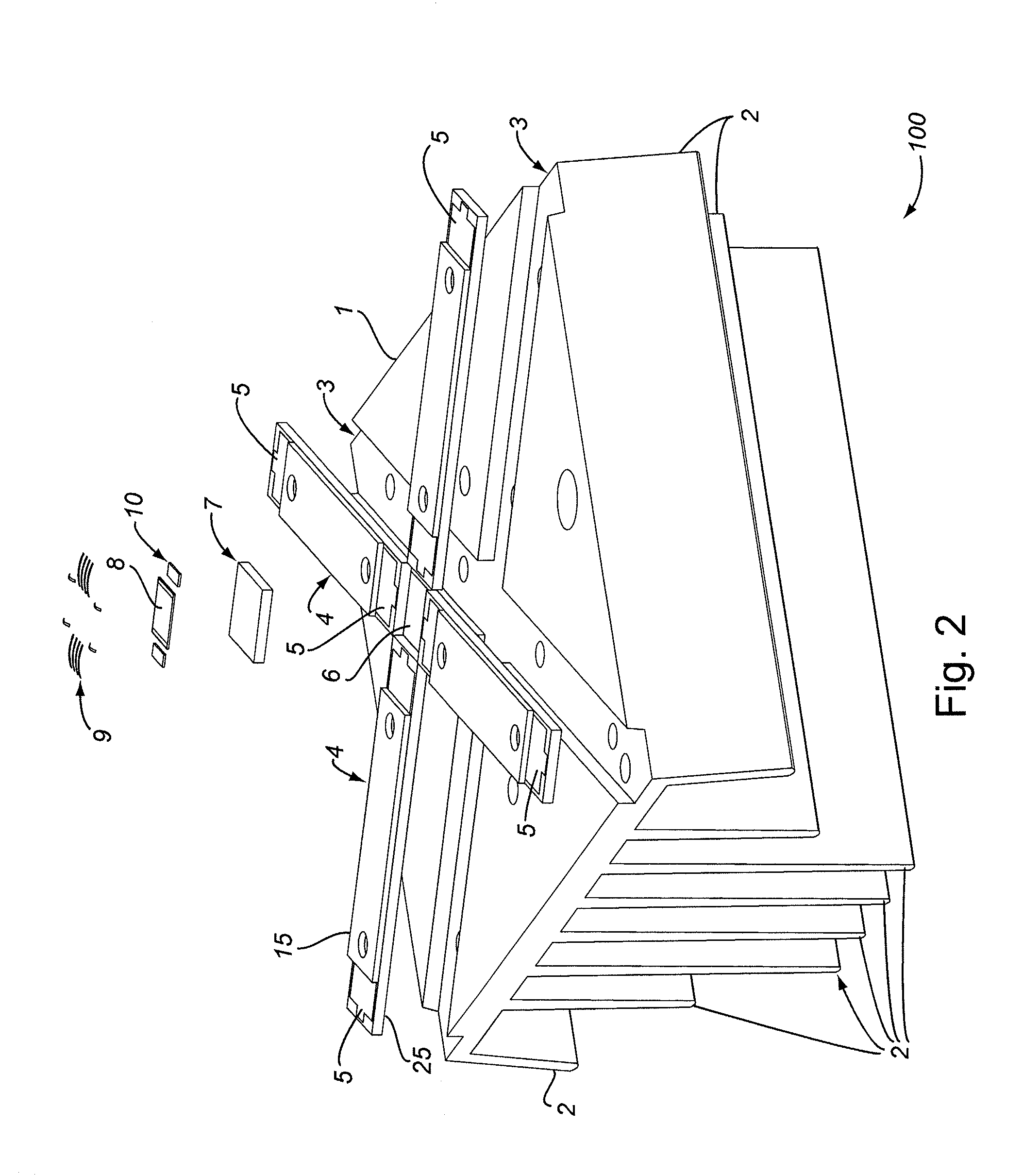
[0039]Referring to FIG. 6, in this embodiment, a single extended substrate-embedded thermally and electrically conductive laminate 11 is attached within the channel 3 along one axis of the heat sink 1, while the channel 3A along the perpendicular axis contains the same conductive tripartite laminates 4 as described above (i.e., terminating proximally near the center of the heat sink). The substrate-embedded laminate 11 and the conductive laminates 4 may be affixed to the channels 3 of heat sink 1 with a variety of thermally-conductive but non-electrically conductive adhesives or mechanical connections (including e.g., epoxy resins, eutectic compositions, solder, cyanoacrylates, mechanical fasters (e.g., conductive, such as metal, or non-conductive, such as plastic), thermosonic bonding, or any combination of the above), although if electrically conductive fasteners (e.g., metal screws) are used, the fasteners must pass through non-conductive regions for...


PUM


Abstract

A device containing a solar cell is provided in the form of a stacked package that has a planar arrangement of conductive laminates at or below the surface of a heat sink. The planar alignment allows placement of electrical connections below the surface of the heat sink and reduces the vertical profile of the device, making it easier to be hermetically sealed. In specific embodiments the solar cell substrate is embedded within the heat sink during the manufacturing phase, eliminating the need for a thermally conductive substrate between the solar cell and the heat sink.

Description

CROSS-REFERENCES TO RELATED APPLICATIONS[0001]This application was filed contemporaneously with U.S. Provisional Application No. 61 / 439,082, filed on Feb. 3, 2011, entitled “INTEGRATED SEMICONDUCTOR SOLAR CELL PACKAGE” and U.S. Provisional Patent Application No. 61 / 439,095, filed on Feb. 3, 2011, entitled “FLEXIBLE HERMETIC SEMICONDUCTOR SOLAR CELL PACKAGE WITH NON-HERMETIC OPTION,” the contents of which are incorporated herein by reference in their entirety.STATEMENT AS TO RIGHTS TO INVENTIONS MADE UNDER FEDERALLY SPONSORED RESEARCH AND DEVELOPMENT[0002]NOT APPLICABLEREFERENCE TO A “SEQUENCE LISTING,” A TABLE, OR A COMPUTER PROGRAM LISTING APPENDIX SUBMITTED ON A COMPACT DISK[0003]NOT APPLICABLEBACKGROUND OF THE INVENTION[0004]This invention relates to packaging for semiconductor photovoltaic devices and specifically for solar cells that are subject to solar-induced heating.[0005]Photovoltaic devices present unique problems requiring specialized packaging to achieve desired levels ...

Claims


Application Information

Patent Timeline
Patent Type & Authority Applications(United States)
IPC IPC(8): H01L31/024H01L31/0203
CPCY02E10/50H01L31/052H01L31/02008
Inventor LAMARCHE, PAUL F.TRIPP, KYLE JEFFREY RUSSO
Owner CACTUS MATERIALS INC
Why Eureka
Try Eureka