Drain Extended Field Effect Transistors and Methods of Formation Thereof

a technology of extended field effect transistor and extended field effect, which is applied in the direction of transistors, semiconductor devices, electrical apparatus, etc., can solve the problems of low device performance, low device performance, and high risk of esd discharge, and achieve the effect of reducing peak doping

Active Publication Date: 2012-08-09
INFINEON TECH AG
View PDF10 Cites 28 Cited by
  • Summary
  • Abstract
  • Description
  • Claims
  • Application Information

AI Technical Summary

Problems solved by technology

In particular, many integrated circuits are highly susceptible to damage from the discharge of static electricity.
The discharge of static electricity, or ESD, has become a critical problem for the electronics industry.
Often, the device is only slightly weakened but is less able to withstand normal operating stresses.
Such a weakened device may result in reliability problems such as increased leakage currents resulting in degraded performance of the device.
In such applications, one challenge is to provide an ESD robust high voltage (HV) transistor element which has excellent mixed signal performance and gate oxide reliability.
However, DeMOS transistors are ESD-weak and require additional protective circuitry to prevent damage from ESD.
Additional ESD circuitry, however, increases the cost of the chip.
However, such a device configuration results into space charge modulation due to localized current distribution and cause a very early thermal failure of the device, which is attributed to filament formation.
As will be described in detail below, this construction results in poor ESD performance requiring additional circuitry to protect the device against ESD damage.

Method used


Image

  • Drain Extended Field Effect Transistors and Methods of Formation Thereof
  • Drain Extended Field Effect Transistors and Methods of Formation Thereof
  • Drain Extended Field Effect Transistors and Methods of Formation Thereof

Examples


Embodiment Construction

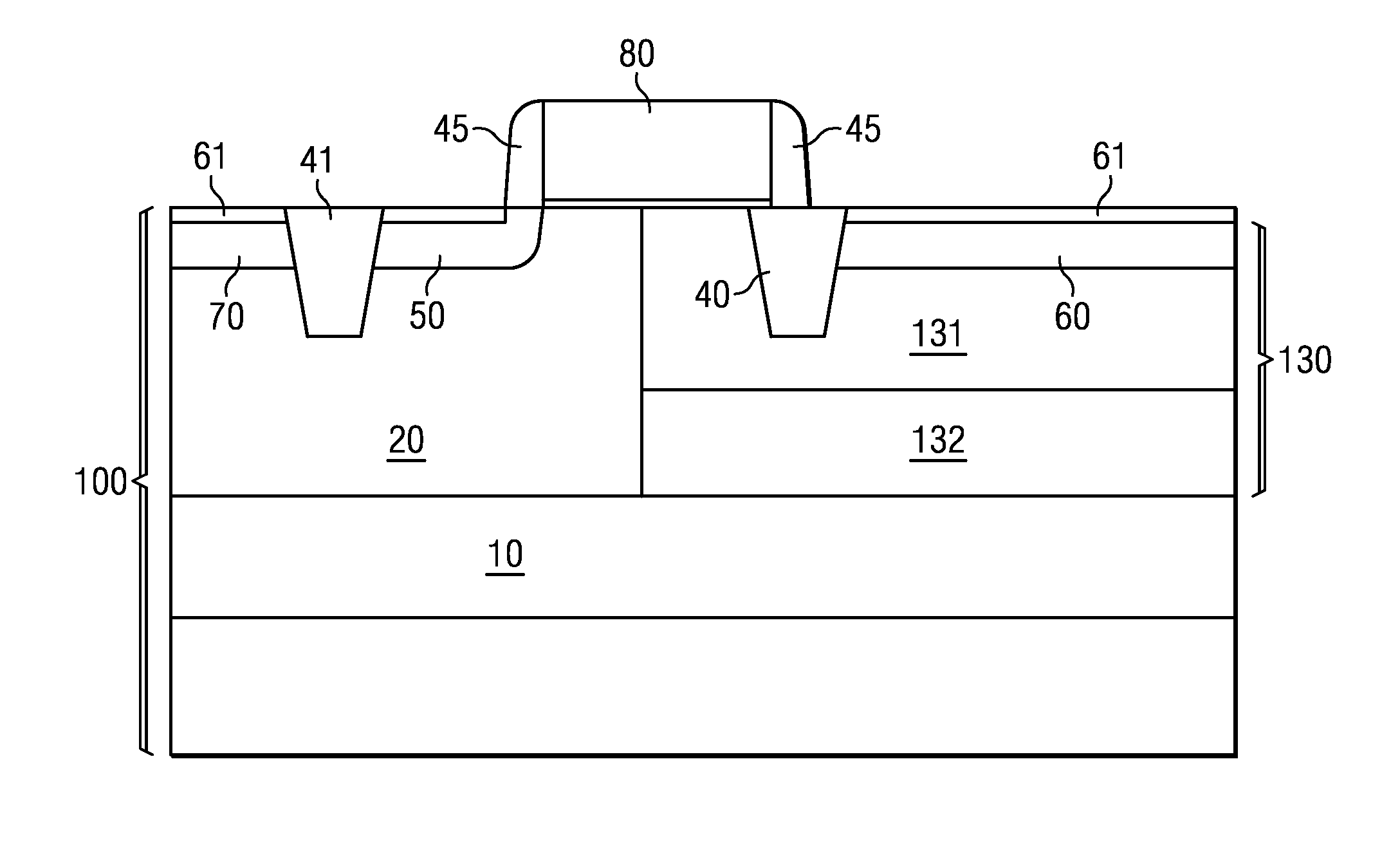
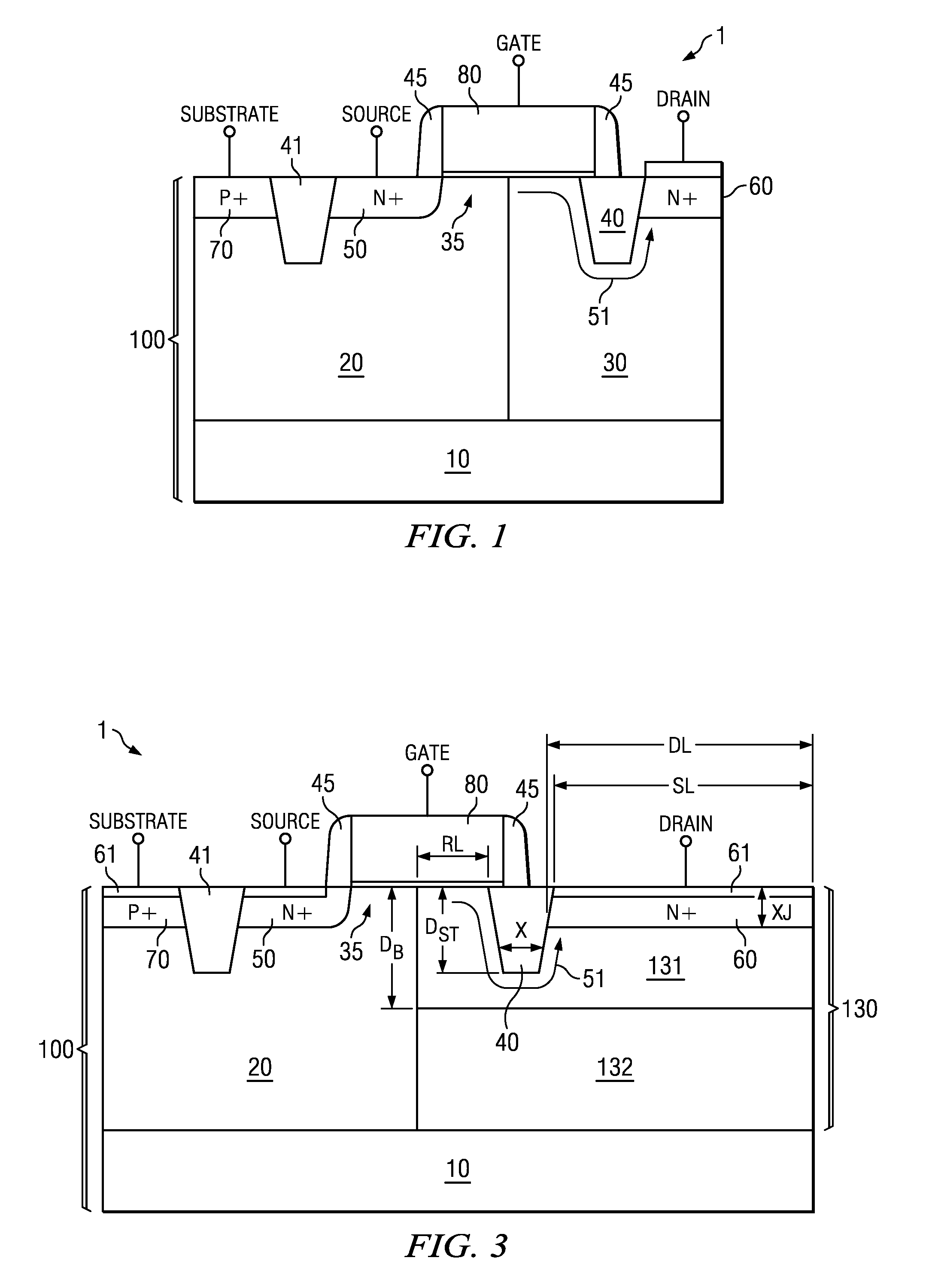
[0033]The making and using of various embodiments are discussed in detail below. It should be appreciated, however, that the present invention provides many applicable inventive concepts that can be embodied in a wide variety of specific contexts. The specific embodiments discussed are merely illustrative of specific ways to make and use the invention, and do not limit the scope of the invention.

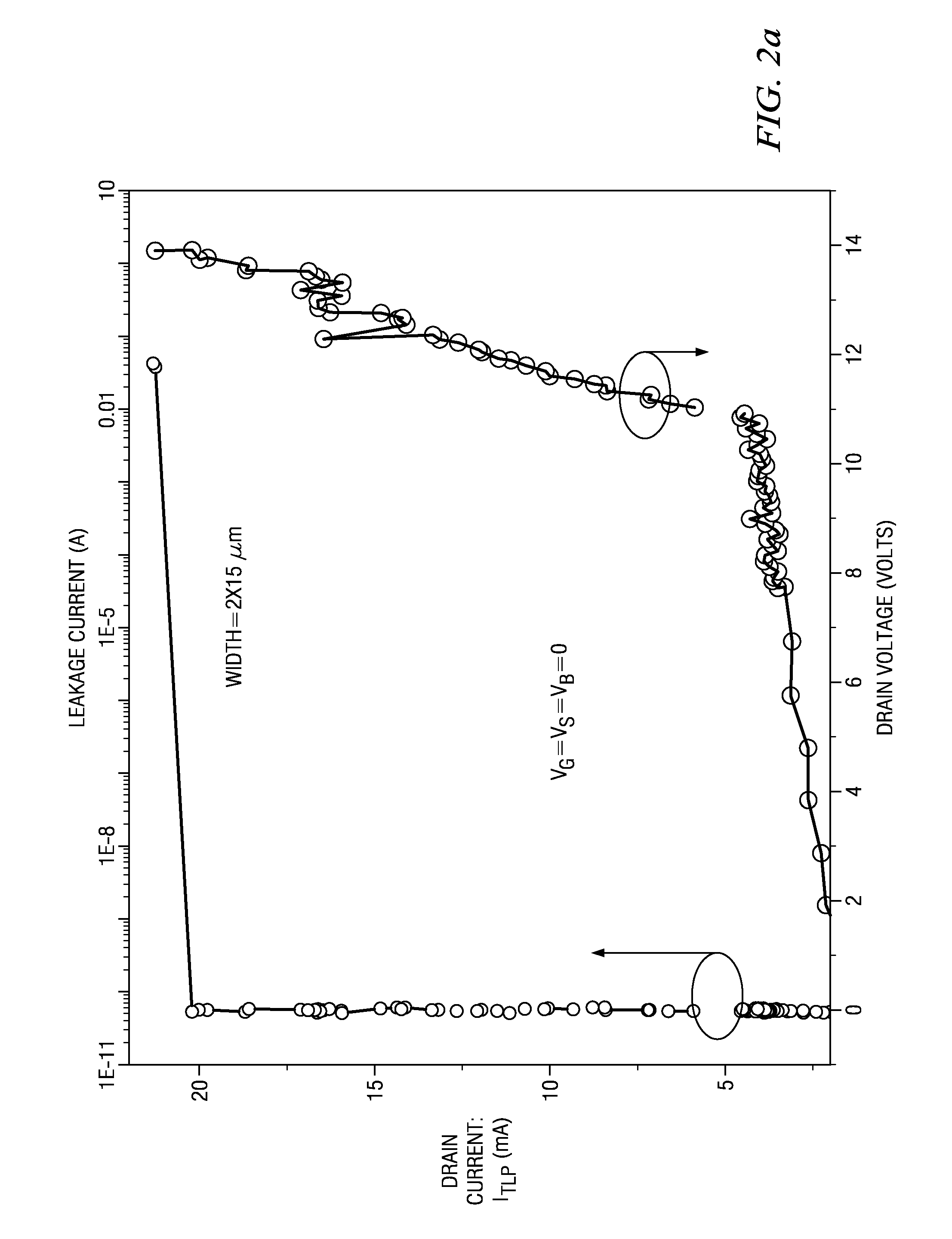
[0034]FIG. 2, which includes FIGS. 2a-2c, illustrates the ESD performance of the device illustrated in FIG. 1, wherein FIG. 2a illustrates experimental performance, and wherein FIGS. 2b-2c illustrates the failure mechanism using device simulation.

[0035]Referring to FIG. 2a, the lower x-axis represents the drain voltage (e.g., voltage in drain region 60 in FIG. 1). The upper x-axis represents the leakage current (sub-threshold leakage and gate leakage) during normal operation of the device after ESD stress. The y-axis represents the drain current ITLP (ESD pulse) used to stress the device. No...


PUM


Abstract

In an embodiment of the invention, a semiconductor device includes a first region having a first doping type, a channel region having the first doping type disposed in the first region, and a retrograde well having a second doping type. The second doping type is opposite to the first doping type. The retrograde well has a shallower layer with a first peak doping and a deeper layer with a second peak doping higher than the first peak doping. The device further includes a drain region having the second doping type over the retrograde well. An extended drain region is disposed in the retrograde well, and couples the channel region with the drain region. An isolation region is disposed between a gate overlap region of the extended drain region and the drain region. A length of the drain region is greater than a depth of the isolation region.

Description

TECHNICAL FIELD[0001]This invention relates generally to semiconductor devices and methods, and more particularly to drain extended field effect transistors and methods of forming thereof.BACKGROUND[0002]As electronic components are becoming smaller and smaller along with the internal structures in integrated circuits, it is becoming easier to either completely destroy or otherwise impair electronic components. In particular, many integrated circuits are highly susceptible to damage from the discharge of static electricity. Generally, electrostatic discharge (ESD) is the transfer of an electrostatic charge between bodies at different electrostatic potentials or voltages, caused by direct contact or induced by an electrostatic field. The discharge of static electricity, or ESD, has become a critical problem for the electronics industry.[0003]Device failures resulting from ESD events are not always immediately catastrophic or apparent. Often, the device is only slightly weakened but i...

Claims


Application Information

Patent Timeline
Patent Type & Authority Applications(United States)
IPC IPC(8): H01L29/772H01L21/336
CPCH01L29/0634H01L29/0653H01L29/0847H01L29/0873H01L29/0878H01L29/1054H01L29/78H01L29/267H01L29/41775H01L29/456H01L29/66659H01L29/7816H01L29/7835H01L29/165H01L29/1095H01L29/66575H01L29/665H01L29/7842H01L21/26513H01L29/45H01L27/088H01L29/0642
Inventor SHRIVASTAVA, MAYANKRUSS, CORNELIUS CHRISTIANGOSSNER, HARALDRAO, RAMGOPAL
Owner INFINEON TECH AG
Why Eureka
Try Eureka