Group iii nitride semiconductor light-emitting device and production method therefor

a technology of nitride semiconductors and light-emitting devices, which is applied in the manufacture of semiconductor/solid-state devices, semiconductor devices, electrical apparatus, etc., can solve the problems of light output reduction and emission performance reduction, and achieve the effect of improving emission performance and high electrostatic breakdown voltag

Inactive Publication Date: 2012-08-16
TOYODA GOSEI CO LTD
View PDF1 Cites 15 Cited by
  • Summary
  • Abstract
  • Description
  • Claims
  • Application Information

AI Technical Summary

Benefits of technology

[0018]The present invention can improve emission performance by controlling the strain in the light-emitting layer or the confinement of the carriers while attaining high electrostatic breakdown voltage.

Problems solved by technology

However, when a pit is formed on an n-type layer and AlGaN is used as a barrier layer of the light-emitting layer, there is the following problem.
When the pit diameter is excessively small, the strain in the light-emitting layer is not sufficiently relaxed, resulting in the reduction of light output.
On the other hand, when the pit diameter is excessively large, the carriers are not sufficiently confined, resulting in the reduction of emission performance.

Method used


Image

  • Group iii nitride semiconductor light-emitting device and production method therefor
  • Group iii nitride semiconductor light-emitting device and production method therefor
  • Group iii nitride semiconductor light-emitting device and production method therefor

Examples


embodiment 1

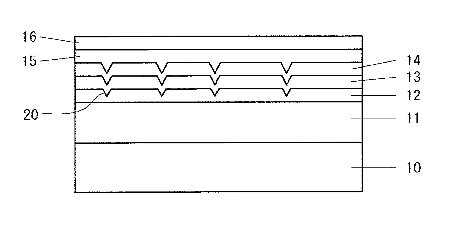
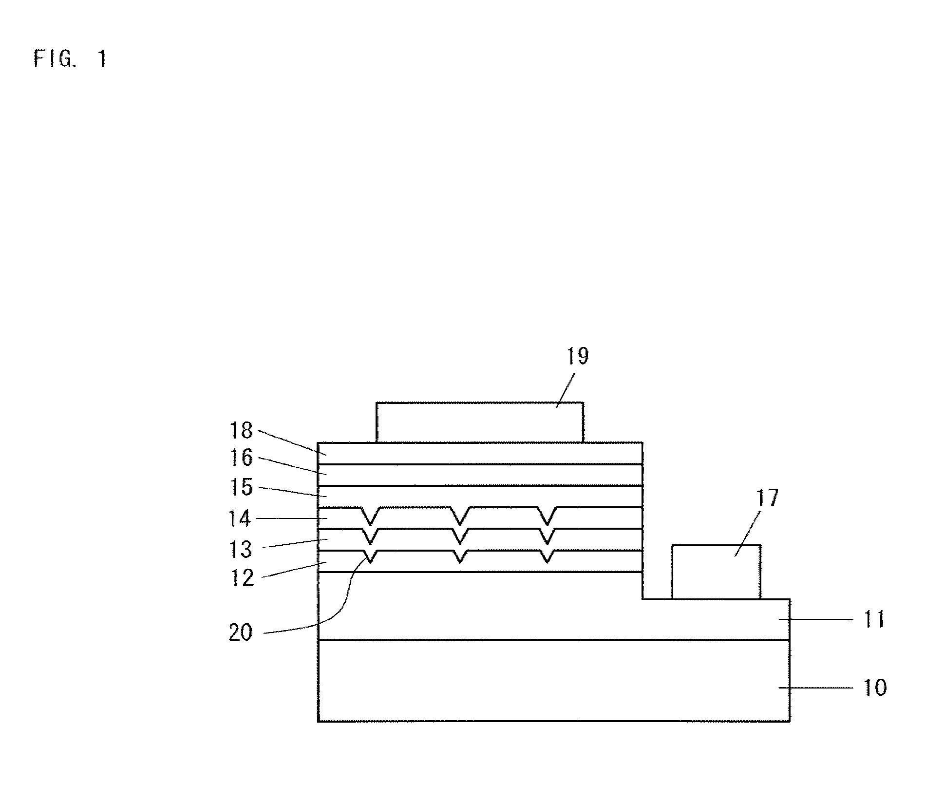
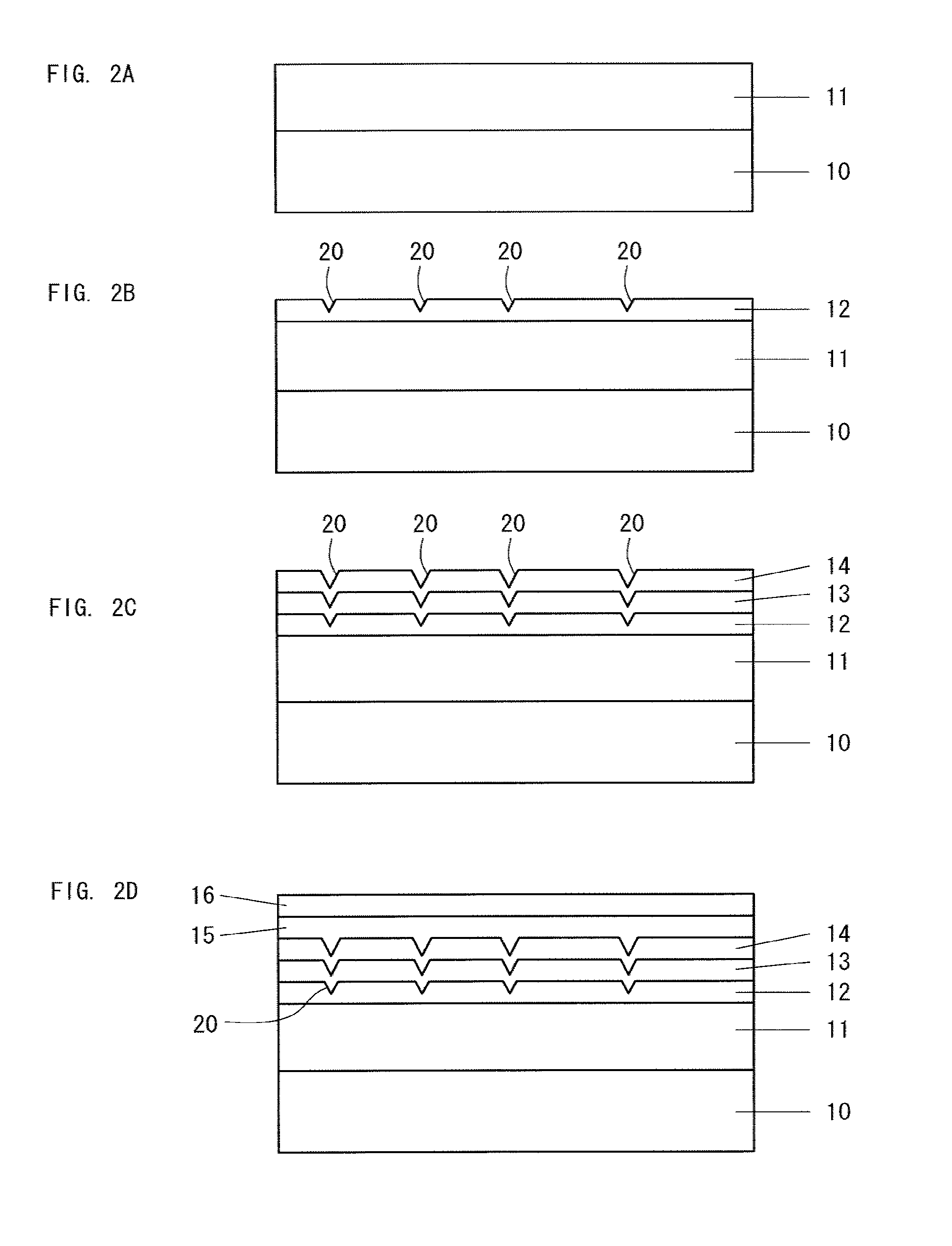
[0026]FIG. 1 shows the configuration of a Group III nitride semiconductor light-emitting device according to Embodiment 1. The Group III nitride semiconductor light-emitting device has a sapphire substrate 10 on which an n-type contact layer 11, an ESD layer 12, an n-type cladding layer 13, a light-emitting layer 14, a p-type cladding layer 15, and a p-type contact layer 16 are sequentially deposited via a buffer layer (not illustrated). A trench with a depth reaching the surface of the n-type contact layer 11 is formed on a portion of the p-type contact layer 16, and an n electrode 17 is formed on the surface of the n-type contact layer exposed by the trench. An ITO transparent electrode 18 is formed on almost the entire surface of the p-type contact layer 16, and a p electrode 19 is formed on the transparent electrode 18.

[0027]A texture including at least one of a dot pattern and a stripe pattern may be formed on the sapphire substrate 10 to improve light extraction efficiency. Th...


PUM

PropertyMeasurementUnit
pit diameteraaaaaaaaaa
temperatureaaaaaaaaaa
diameteraaaaaaaaaa

Abstract

The present invention provides a Group III nitride semiconductor light-emitting device exhibiting improved emission performance and high electrostatic breakdown voltage. The Group III nitride semiconductor light-emitting device has a layered structure in which an n-type contact layer, an ESD layer, an n-type cladding layer, a light-emitting layer, a p-type cladding layer, and a p-type contact layer are deposited on a sapphire substrate. The ESD layer has a pit. The n-type cladding layer and the light-emitting layer are formed without burying the pit. The pit has a diameter of 110 nm to 150 nm at an interface between the n-type cladding layer and the light-emitting layer. The barrier layer of the light-emitting layer is formed of AlGaN having an Al composition ratio of 3% to 7%.

Description

BACKGROUND OF THE INVENTION[0001]1. Field of the Invention[0002]The present invention relates to a Group III nitride semiconductor light-emitting device exhibiting improved emission performance and high electrostatic breakdown voltage due to strain relaxation in a light-emitting layer by forming a pit on an n-type layer, wherein AlGaN is used as a barrier layer of the light-emitting layer.[0003]2. Background Art[0004]As a Group III nitride semiconductor light-emitting device, a structure has been known in which a pit is formed on an n-type layer, and a light-emitting layer is formed without burying the pit.[0005]For example, Japanese Patent Application Laid-Open (kokai) No. 2007-180495 discloses that an ESD layer comprising two layers: i-GaN layer and n-GaN layer, is provided on an n contact layer, a pit is formed on the i-GaN layer, and Si concentration and film thickness of the n-GaN layer are controlled to fall within a specified range, thereby high electrostatic breakdown voltag...

Claims


Application Information

Patent Timeline
Patent Type & Authority Applications(United States)
IPC IPC(8): H01L33/04H01L33/02
CPCH01L33/24H01L33/007
Inventor NAKAMURA, RYO
Owner TOYODA GOSEI CO LTD
Why Eureka
Try Eureka