Nanotubes cold cathode

Inactive Publication Date: 2005-07-07
NANO
View PDF12 Cites 22 Cited by
  • Summary
  • Abstract
  • Description
  • Claims
  • Application Information

AI Technical Summary

Problems solved by technology

The problem with these technologies is that the nanotubes are grown in a separate reactor, harvested and than attached to a substrate using various means.
These technologies generally do not produce good results and do not lead to a process that is manufacturable.
Because of this, one is limited to a thermal CVD method of fabricating the nanotubes, directly on the substrate.
The problem wit

Method used


Image

  • Nanotubes cold cathode
  • Nanotubes cold cathode
  • Nanotubes cold cathode

Examples


Embodiment Construction

Overview

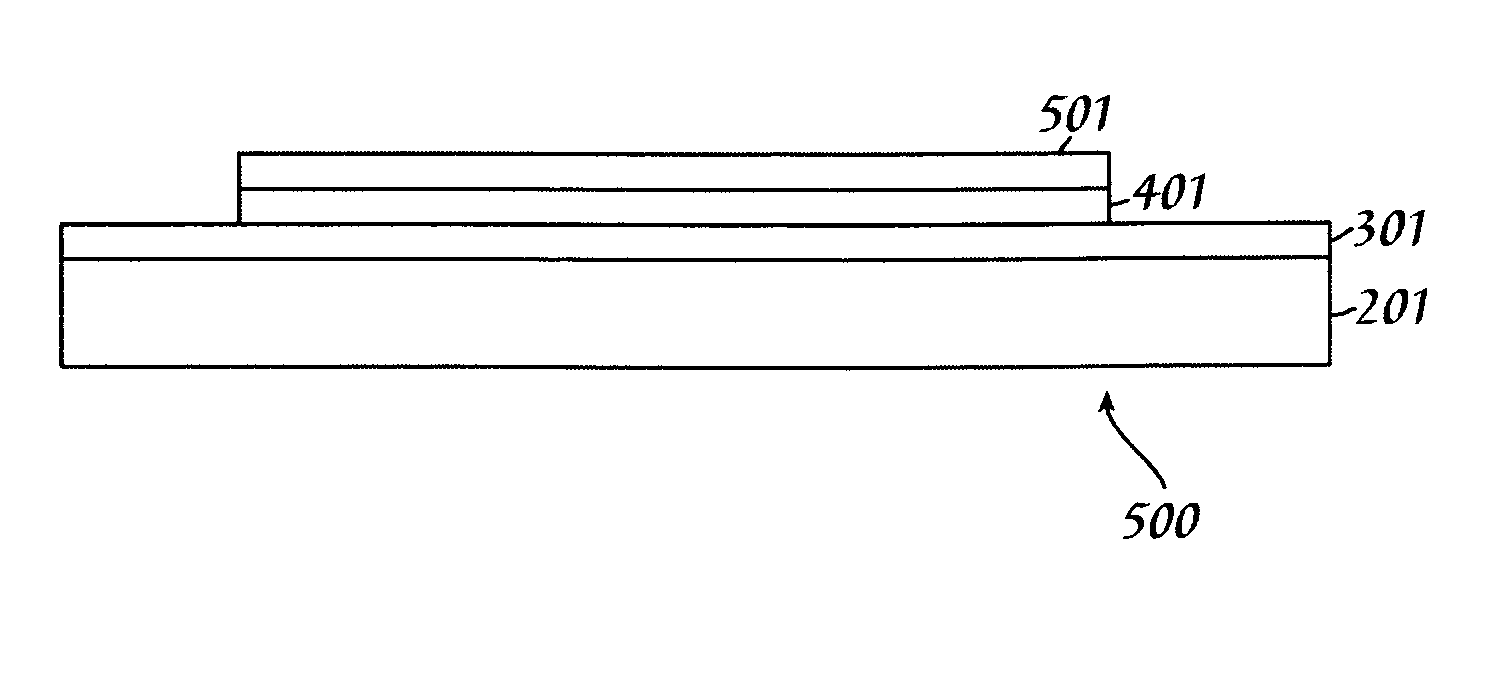
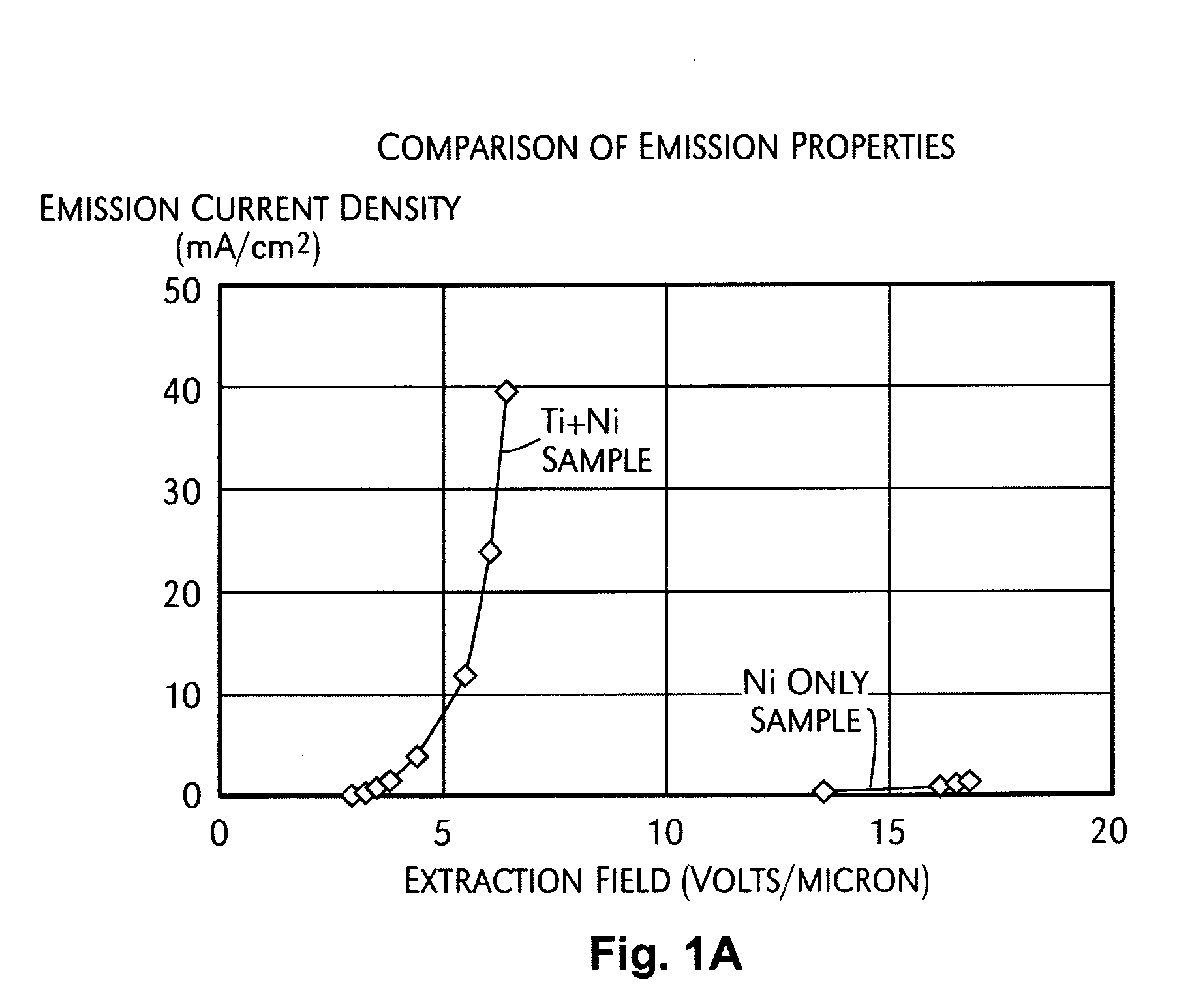
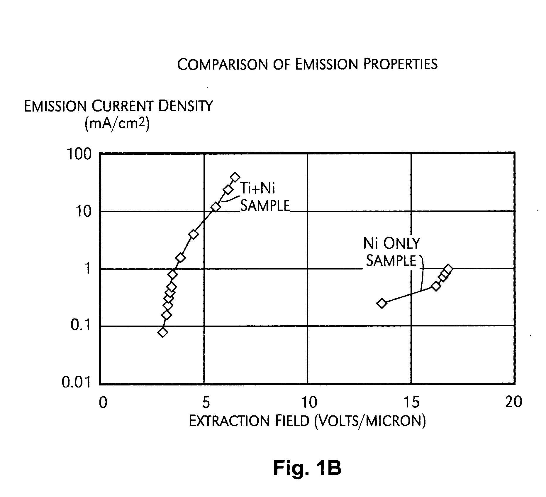
[0017] The present invention addresses the foregoing problems. The present invention demonstrates a carbon nanotube field emitter that is grown by thermal CVD using a Ni catalytic film that was deposited on an adhesion layer of Ti between the Ni film and the forsterite ceramic substrate. Several experiments were tried in which two samples were placed side by side in a thermal CVD reactor. Hydrogen (H2) and ethylene (C2H4) were used in the reactor to form the carbon film. On one substrate, a 1000 A layer of Ni was deposited directly onto clean forsterite (a ceramic material). On the other substrate, 1000 A of titanium (Ti) was deposited directly on the clean forsterite surface and then 1000 A of Ni was deposited on top of the Ti layer. The Ni was deposited by e-beam evaporation in the same deposition run for each substrate, so the Ni layer thickness is identical. Thus, since they were run side-by-side in the reactor and the only substrate fabrication difference was that one...


PUM


Abstract

A two-layer approach is provided for thermally growing carbon nanotubes on a substrate for field emitter applications. An adhesion layer is deposited on a cathode. A catalyst layer is then deposited on the adhesion layer, and then a carbon nanotube film is grown on the catalyst layer.

Description

TECHNICAL FIELD [0001] The present invention relates in general to field emission devices, and in particular, to field emission devices using carbon nanotubes. BACKGROUND INFORMATION [0002] Carbon nanotubes are carbon fibers or rods that can be very long and very narrow. The length can be on the order of microns or tens of microns, the width on the order of nanometers, so the aspect ratio of height to width can be very high. Carbon nanotubes fall into a class of carbon materials called fullerenes. The tubes can have a single wall or multiple walls of carbon layers, the layers are similar to a sheet of graphite wrapped in a tube form. Nanotubes were first identified by S. lijima [S. lijima, Nature (London) Vol. 354, page 56, 1991. Nanotubes can be grown by several methods that fall into 3 categories. [0003] 1. Laser Vaporization Synthesis Method. This method involves the vaporization of a carbon rod by a laser in a high temperature argon environment. This method produces a felt-like ...

Claims


Application Information

Patent Timeline
IPC IPC(8): H01J9/02
CPCB82Y10/00H01J2201/30469H01J9/025
Inventor YANIV, ZVIFINK, RICHARDHUTCHINS, DEANYANG, MOHSHITHUESEN, LEIF
Owner NANO
Why Eureka
Try Eureka