Epitaxial material used for GAN based LED with low polarization effect and manufacturing method thereof

Active Publication Date: 2009-09-24
INST OF PHYSICS - CHINESE ACAD OF SCI
View PDF9 Cites 20 Cited by
  • Summary
  • Abstract
  • Description
  • Claims
  • Application Information

AI Technical Summary

Benefits of technology

[0041]The present invention avoids problems of several conventional technology of growing non-polarized GaN material, for example, poor thermal stability of γ-LiAlO2 and high dopant concentration of the grown GaN material background, and severe non-symmetry of grown A-plane GaN epitaxial material on R-plane substrate of sapphire, which results in difficulty for growing epitaxial material in two-dimensional layer status.
[0042]The present invention adopts combination of regulating and controlling quantum well structure and quantum well active region structure to enable the energy band of the quantum well active region to bend in inversed direction by energy band engineering, which actually lowers polarization effect of the quantum well active region, so as to achieve low polarization effect of the quantum well active region, increase overlapping of electron or hole wave function, and increase the concentration of the electron or hole to further increase the light emission effect of the inner quantum of the LED, because the electron or hole of the regulating and controlling quantum well region tunnels into the quantum well active region.
[0043]The conventional GaN based LED quantum well active region has problems of high intensity built-in electric field caused by strong polarization effect, red-shift of light emission wavelength caused by spatial separation of positive and negative charge carrier, and the even worse result of reducing overlapping of electron and hole wave function and greatly lowering light emission efficiency of the material, but the present invention provides the method for manufacturing an epitaxial material for GaN based LED with low polarization effect to solve these problems.
[0044]The present invention provides an epitaxial material for GaN based LED with low polarization effect, wherein the thickness and In composition of the InAlGa

Problems solved by technology

Because III-V Nitride material has a spatial structure without space inversion symmetry, and the electronegativity of atom of V group elements is far different from that of N, there is a strong polarization along of GaN, thus the polarization effect will generate a built-in electric field with rather high intensity, and spatially separate positive and negative charge carriers, which results in red shift of emission wavelength, and even worse reduction in wave function overlap of electron and hole, so as to greatly decrease the light emission efficiency of the material.
Because of the poor crystal quality of GaN, its dislocation density reaches 108-1010/cm−2, and its strong polarization effect severely restrains the light emission efficiency of LED.
The current main aspect believes that existence of In component results in a localization effect, which in turn incre

Method used


Image

  • Epitaxial material used for GAN based LED with low polarization effect and manufacturing method thereof
  • Epitaxial material used for GAN based LED with low polarization effect and manufacturing method thereof

Examples


embodiment 1

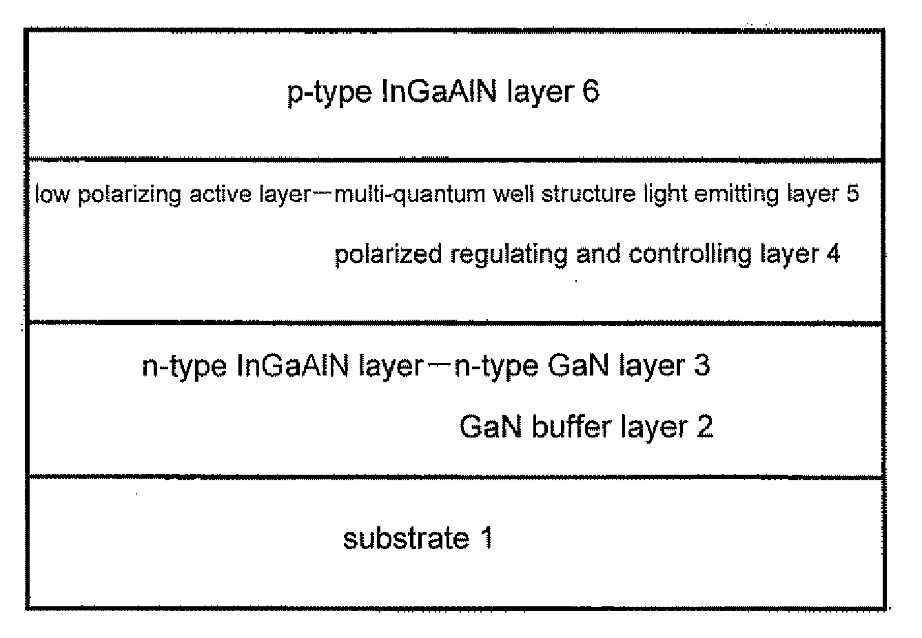
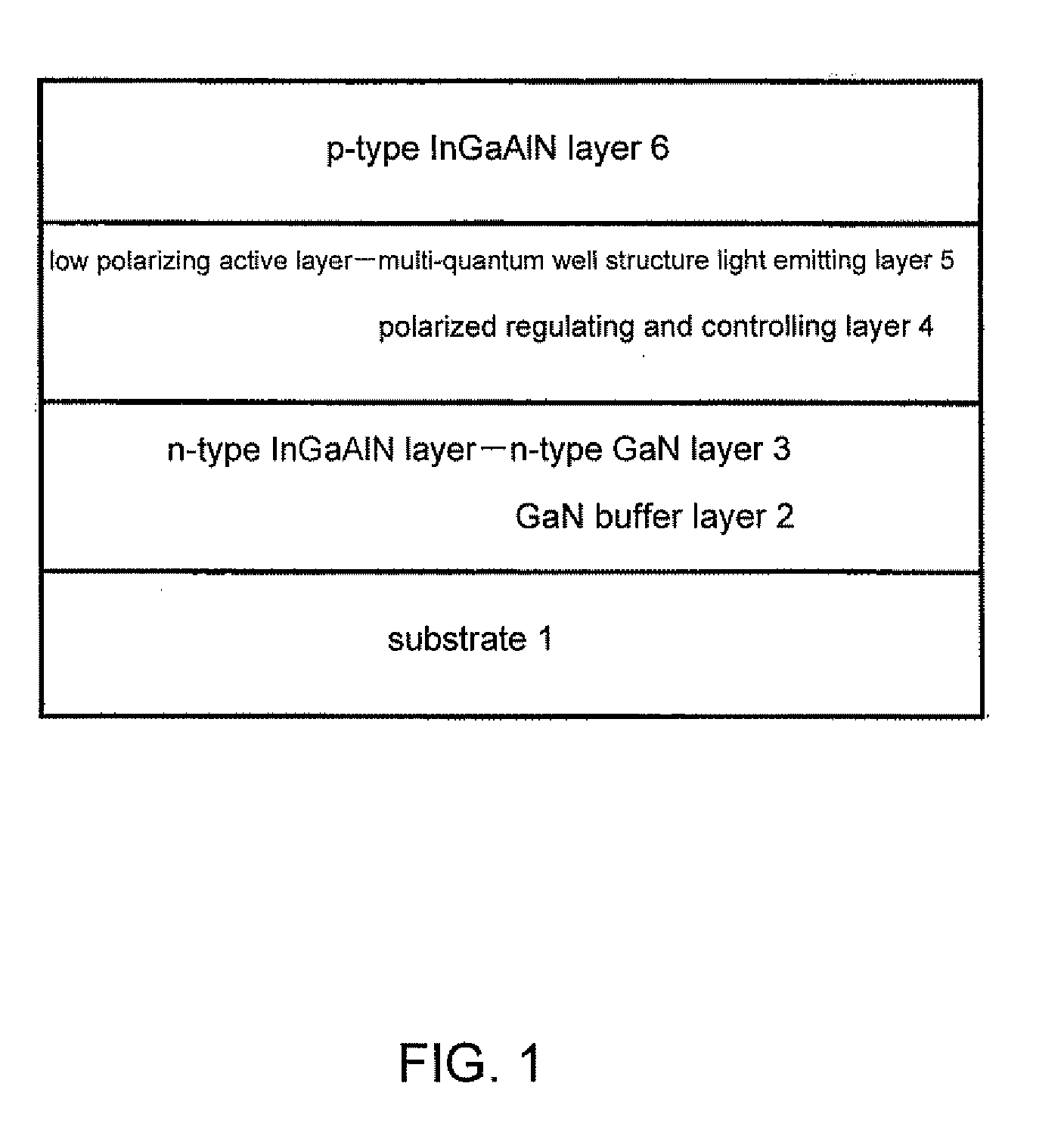
[0050]The epitaxial material used for GaN based LED with low polarization effect is manufactured by using the method of the present invention, the method particularly comprises steps of:

[0051]adopting sapphire with a thickness of 0.43 mm as substrate 1; growing in turn on the substrate 1 by metal organic chemical vapor phase deposition (MOCVD) technology a GaN buffer layer 2 (composed of GaN) with a thickness of 10 nm, an n-type GaN layer 3 (composed of GaN) with a thickness of 2500 nm, an InGaN multi-quantum well structure polarized regulating and controlling layer 4 (a multi-quantum well structure with 2 periodicities composed of a GaN barrier layer and an In0.15Ga0.85N quantum well layer, wherein the GaN barrier layer has a thickness of 10 nm, the In0.15Ga0.85N quantum well layer has a thickness of 3.5 nm, dopant concentration of said GaN barrier layer is 0, dopant concentration of said In0.15Ga0.85N quantum well layer is 1×10¹⁸ / cm3, and corresponding peak of theoretical design l...

embodiment 2

[0052]The epitaxial material used for GaN based LED with low polarization effect is manufactured by using the method of the present invention, the method particularly comprises steps of:

[0053]adopting SiC with a thickness of 0.4 mm as substrate 1; growing in turn on the substrate 1 by metal organic chemical vapor phase deposition (MOCVD) technology a GaN buffer layer 2 (composed of AlN) with a thickness of 200 nm, an n-type GaN layer 3 with a thickness of 1 μm, an InGaN multi-quantum well structure polarized regulating and controlling layer 4 (a quantum well structure with 1 periodicity composed of a GaN barrier layer and an In0.12Ga0.88N quantum well layer, wherein the GaN barrier layer has a thickness of 10 nm, the In0.12Ga0.88N quantum well layer has a thickness of 4 nm, dopant concentration of said GaN barrier layer is 0, dopant concentration of said In0.12Ga0.88N quantum well layer is 1×10¹⁸ / cm3, and corresponding peak of theoretical design light photon energy is 2.4 eV), an In...

embodiment 3

[0054]The epitaxial material used for GaN based LED with low polarization effect is manufactured by using the method of the present invention, the method particularly comprises steps of:

[0055]adopting sapphire with a thickness of 0.43 mm as substrate 1; growing in turn on the substrate 1 by metal organic chemical vapor phase deposition (MOCVD) technology a GaN buffer layer 2 (composed of AlN) with a thickness of 100 nm, an n-type GaN layer 3 with a thickness of 1 μm, an InGaN multi-quantum well structure polarized regulating and controlling layer 4 (a multi-quantum well structure with 5 periodicities composed of an In0.05Ga0.95N barrier layer and an In0.13Ga0.87N quantum well layer, wherein the In0.05Ga0.95N barrier layer has a thickness of 10 nm, the In0.13Ga0.87N quantum well layer has a thickness of 4 nm, dopant concentration of said GaN barrier layer is 0, dopant concentration of said In0.13Ga0.87N quantum well layer is 5×10¹⁷ / cm3, and corresponding peak of theoretical design li...


PUM


Abstract

A method of manufacturing epitaxial material used for GaN based LED with low polarization effect, which includes steps of growing n-type InGaAlN layer composed of GaN buffer layer (2) and n-type GaN layer (3), low polarizing active layer composed of InGaAlN multi-quantum well structure polarized regulating and controlling layer (4) and InGaAlN multi-quantum well structure light emitting layer (5) and p-type InGaAlN layer (6) on sapphire or SiC substrate (1) in turn. The method adds InGaAlN multi-quantum well structure polarized regulating and controlling layer, thus reduces polarization effect of quantum well active region.

Description

BACKGROUND OF THE INVENTION[0001]1. Field of the Invention[0002]The present invention relates to an epitaxial material used for GaN based LED and a method for manufacturing the same, particularly to an epitaxial material used for GaN based LED with low polarization effect by using quantum well regulating and controlling technology to reduce the polarization effect and a method for manufacturing the same.[0003]2. Description of the Related Art[0004]Wide-bandgap materials with GaN as a representative are third generation semiconductors successive of Si and GaAs semiconductors, which is developed rapidly in the nineties of the last century due to the breakthrough of the epitaxial growing technology. Within less than ten years, GaN becomes a very hot subject for study worldwidely, while the LED possesses a major part among the GaN market. Presently, it had been already industrialized to utilize C-plane and A-plane sapphire substrate for fabricating GaN based LED. Normally we use epitaxi...

Claims


Application Information

Patent Timeline
IPC IPC(8): H01L29/15H01L21/20H01L33/00H01L33/04H01L33/06
CPCB82Y20/00H01L33/06H01L33/04H01L33/007Y10S438/956
Inventor CHEN, HONGJIA, HAIQIANGGUO, LIWEIWANG, WENXINZHOU, JUNMING
Owner INST OF PHYSICS - CHINESE ACAD OF SCI
Why Eureka
Try Eureka