MOCVD epitaxy processing method of AlInGaN quaternary alloy thin-film material

A technology for quaternary alloys and thin film materials, which is applied in the fields of electrical components, semiconductor/solid-state device manufacturing, circuits, etc., can solve the problems of AlInGaN quaternary alloy material growth and preparation difficulties, lattice matching offset, and different bond lengths and bond energies. , to achieve the effect of improving migration ability and metal element incorporation efficiency, highly matching lattice constant, and uniform distribution of metal elements

Inactive Publication Date: 2014-04-09
南京大学扬州光电研究院
View PDF2 Cites 9 Cited by
  • Summary
  • Abstract
  • Description
  • Claims
  • Application Information

AI Technical Summary

Problems solved by technology

[0003] AlInGaN quaternary alloy materials and their application in quantum well structures have made considerable progress, but the growth and preparation of high-quality AlInGaN quaternary alloy materials is still relatively difficult, specifically reflected in: 1. GaN-based binary alloy material systems Different materials have different bond length and bond energy, poor mutual solubility, huge difference in decomposition temperature, and desorption of elements during the growth process, which lead to AlInGaN material alloy composition easily deviating from the lattice-matched composition value, and with the increase of growth temperature , AlInGaN quaternary alloy material disorder process intensifies and induces component

Method used


Image

  • MOCVD epitaxy processing method of AlInGaN quaternary alloy thin-film material
  • MOCVD epitaxy processing method of AlInGaN quaternary alloy thin-film material
  • MOCVD epitaxy processing method of AlInGaN quaternary alloy thin-film material

Examples


Embodiment Construction

[0015] Production equipment and materials:

[0016] 1. Metal organic chemical vapor deposition MOCVD satellite disk 2-inch 11-chip preparation system.

[0017] 2. Metal-organic MO growth source: trimethylgallium (TMGa), trimethylaluminum (TMAl), and trimethylindium (TMln1, TMln2) are respectively used as sources of gallium, aluminum, and indium in the quaternary alloy AlInGaN material.

[0018] 3. Ammonia (NH 3 ), as a nitrogen source.

[0019] 4. MO source intake auxiliary gas path.

[0020] The MO growth source, ammonia gas and auxiliary gas path are input into the MOCVD reaction chamber through independent pipelines and independent systems.

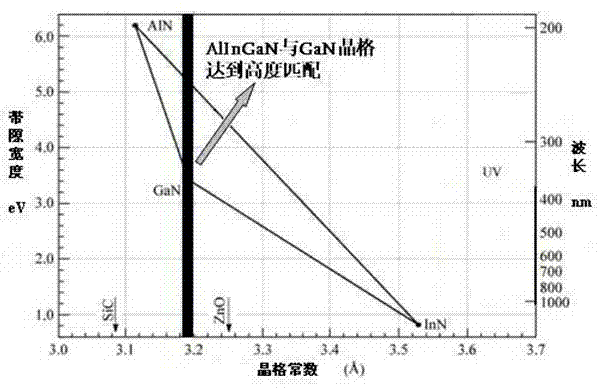
[0021] By adjusting the process parameters such as MOCVD MO source flow, growth temperature, and pressure, the MOCVD MO source flow setting meets: TMA / TMI=4.66, which achieves a high degree of matching with the in-plane lattice constant of the GaN material.

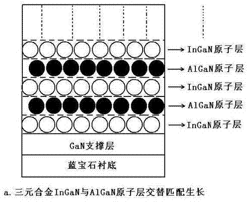
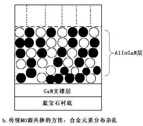
[0022] Such as figure 1 As shown, by adjusting the MO source flow rate t...


PUM


Abstract

An MOCVD epitaxy processing method of an AlInGaN quaternary alloy thin-film material belongs to the technical field of semi-conductors. The AlInGaN quaternary alloy thin-film material is formed by virtue of using a metal organic chemical vapor deposition (MOCVD) epitaxy technology and employing a method of alternatively matching and growing ternary alloy InGaN and AlGaN materials in a thickness of atomic level. The AlInGaN quaternary alloy thin-film material prepared by using the aforementioned technology can achieve the following parameter indexes: (1) the half-peak height and width of an X-ray diffraction (XRD) (002) symmetry plane < 240 seconds; (2) the material surface roughness < 1 nm; and (3) the c-face lattice constant mismatch degree with respect to GaN < 0.5%.

Description

technical field [0001] The invention relates to an epitaxial growth process method for aluminum indium gallium nitrogen (AlInGaN) quaternary alloy thin film materials, and belongs to the technical field of semiconductors. Background technique [0002] Light-emitting diode (LED) devices have made rapid progress in recent years, and have been widely used in consumer electronics products and various types of indicating light sources. However, the luminous performance of LED devices is still restricted by the internal quantum efficiency of its quantum wells, such as the polarization effect of materials and the preparation of high-quality quantum well structures. Studies have shown that the photoelectric performance of light-emitting diodes can be effectively improved by using the quaternary alloy AlInGaN thin film material as the barrier layer material of the LED quantum well structure. AlInGaN material has the following advantages: the lattice constant can be adjusted independ...

Claims


Application Information

Patent Timeline
IPC IPC(8): H01L21/205H01L33/32
CPCH01L21/0254H01L21/0262H01L33/0075
Inventor 徐峰陈鹏谭崇斌徐洲张琳吴真龙高峰徐兆青邵勇王栾井宋雪云
Owner 南京大学扬州光电研究院
Why Eureka
Try Eureka