P-type gate enhanced HEMT device and manufacturing method thereof

A manufacturing method and enhanced technology, which is applied in semiconductor/solid-state device manufacturing, semiconductor devices, electrical components, etc., can solve problems such as difficult process control, current collapse, and saturation current drop, and solve the problems of difficult process control and current collapse Improvement, off-state leakage reduction effect

Inactive Publication Date: 2018-12-07
SUZHOU NENGWU ELECTRONICS TECH
View PDF3 Cites 10 Cited by
  • Summary
  • Abstract
  • Description
  • Claims
  • Application Information

AI Technical Summary

Problems solved by technology

Use p-GaN to increase the potential barrier at the AlGaN/GaN interface channel to above the Fermi level, so that the conductive channel under the gate is disconnected, the two-dimensional electron gas is exhausted, and the enhancement mode is realized; the realized device needs It is difficult to etch the p-GaN with a thickness of tens of nanometers outside the gate, and the process control is difficult and the repeatability is poor; the etching is easy to generate interface states, which will lead to aggravated device current collapse and affect device performance
figure 2 The enhancement-mode HEMT with selective area epitaxy p-GaN shown in , which uses p-GaN to enhance the AlGaN/GaN The potential barrier at the interface channel is above the Fermi level, so that the conductive channel under the gate is disconnected, the two-dimensional electron gas is exhausted, and the enhancement mode is realized; the enhancement mode device realized by it has a low threshold value, and it is difficult to achieve high Devices with a threshold voltage; process implementation is difficult, and epitaxial quality is not high; epitaxial p-GaN sidewalls are not steep, which affects subsequent processes
image 3 The hydrogen-passivated p-GaN enhancement-mode HEMT shown in , which depletes the two-dimensional electron gas below the gate by

Method used


Image

  • P-type gate enhanced HEMT device and manufacturing method thereof
  • P-type gate enhanced HEMT device and manufacturing method thereof
  • P-type gate enhanced HEMT device and manufacturing method thereof

Examples


Embodiment 1

[0090] A method for manufacturing a p-type gate enhanced HEMT device, comprising the steps of:

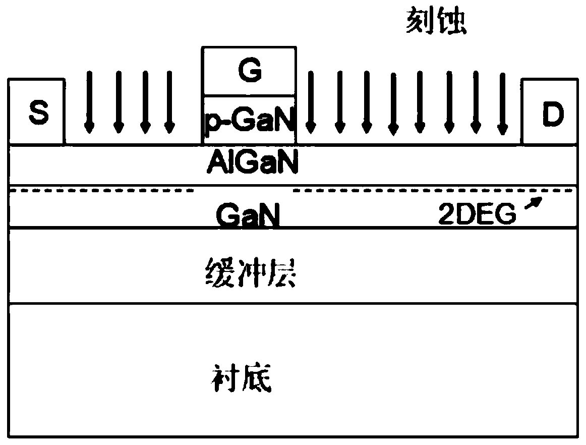
[0091] 1) Grown by metal organic compound chemical vapor deposition (MOCVD) such as Figure 5 The epitaxial structure shown; the substrate is made of Si with a thickness of 400 μm, the buffer layer is made of high-resistance GaN with a thickness of 4200 nm, the thickness of GaN in the AlGaN / GaN heterostructure is 260 nm, and the thickness of AlGaN is 18 nm. The content of Al components in AlGaN is 18%, and the thickness of p-GaN is 70nm;

[0092] 2) Plasma etching is used to remove the p-GaN in the source region and the drain region, and the device structure after etching is as follows Figure 6 As shown; the etching area can be determined by photolithography, and the specific steps of photolithography include pretreatment, uniform glue, pre-baking, exposure and development;

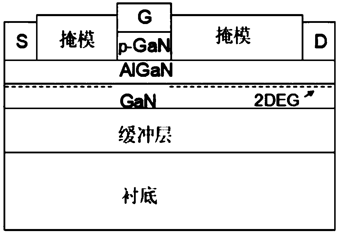
[0093] 3) Deposit Ti / Al / Ni / Au on the source region and the drain region by electron beam evaporation as ...

Embodiment 2

[0098] A method for manufacturing a p-type gate enhanced HEMT device, comprising the steps of:

[0099] 1) The substrate / buffer layer / AlGaN / GaN heterostructure / high-resistance GaN epitaxial structure is grown by metal-organic compound chemical vapor deposition (MOCVD); the substrate is made of Si with a thickness of 400 μm, and the buffer layer is made of high-resistance GaN , the thickness is 4200nm, the thickness of GaN in AlGaN / GaN heterostructure is 260nm, the thickness of AlGaN is 18nm, the content of Al component in AlGaN is 18%, and the thickness of high resistance GaN is 70nm;

[0100] 2) Use plasma etching to remove the high-resistance GaN in the source region and the drain region. The etching region can be determined by photolithography. The specific steps of photolithography include pretreatment, glue leveling, pre-baking, exposure and development;

[0101] 3) Deposit Ti / Al / Ni / Au on the source region and the drain region by electron beam evaporation as the source el...

Embodiment 3

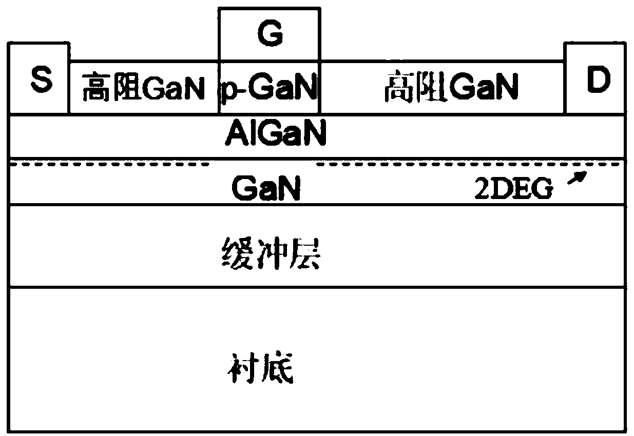
[0106] The manufacturing method of the p-type gate-enhanced HEMT device in this embodiment is basically the same as that in Embodiment 1, the difference is that after the source electrode and the drain electrode are prepared, the gate electrode can be prepared first, and then the etching process is used The p-GaN between the gate electrode and any one of the source electrode and the drain electrode is thinned, and finally the thinned p-GaN is passivated to form high-resistance GaN.


PUM

PropertyMeasurementUnit
Thicknessaaaaaaaaaa
Thicknessaaaaaaaaaa
Thicknessaaaaaaaaaa

Abstract

The invention discloses a P-type gate enhanced HEMT device and a manufacturing method thereof. The method comprises steps that a heterojunction is manufactured, a gate, a source and a drain matched with the heterojunction are manufactured, a third semiconductor is formed on the heterojunction, the third semiconductor in the non-gate region is thinned, the third semiconductor in the non-gate regionis then converted into a fourth semiconductor, the third semiconductor in the gate region is retained, and the fourth semiconductor is a high-resistance semiconductor. The manufacturing method is advantaged in that no secondary extension is required, etching the gate region of the device is further not required, uniformity, repeatability and introduction of damage caused in the etching process are avoided, partial etching is performed on an active region besides the gate region of the device, and damage is reduced.

Description

technical field [0001] The invention relates to an enhanced HEMT device, in particular to a p-type gate enhanced HEMT device and a manufacturing method thereof, belonging to the technical field of semiconductor electronic switching devices. Background technique [0002] Group III nitride semiconductors are an important representative of the third-generation semiconductor materials. Compared with the first-generation and second-generation semiconductor materials, they have the advantages of large band gap, high breakdown electric field, high electron mobility and high saturation electron velocity. Therefore, group III nitride semiconductors have broad application prospects in the fields of industry, power systems, transportation, communications, and consumer electronics. Group III nitride semiconductor heterostructures, taking AlGaN / GaN heterojunction as an example, because the polarization effect can produce high concentration (>10 13 cm -2 ) and high electron mobility ...

Claims


Application Information

Patent Timeline
IPC IPC(8): H01L21/335H01L29/778H01L29/06
Inventor 张宝顺徐宁杜仲凯
Owner SUZHOU NENGWU ELECTRONICS TECH
Why Eureka
Try Eureka