Light-Emitting Element, Display Device, Lighting Device, and Method for Manufacturing the Same

a technology of light-emitting elements and display devices, which is applied in the direction of photovoltaic energy generation, electrical apparatus, semiconductor devices, etc., can solve the problems of insufficient element characteristics of conventional light-emitting elements and need further improvement, so as to reduce the driving voltage and improve the element characteristics. , the effect of reducing the voltage loss

Active Publication Date: 2012-08-16
SEMICON ENERGY LAB CO LTD
View PDF24 Cites 30 Cited by
  • Summary
  • Abstract
  • Description
  • Claims
  • Application Information

AI Technical Summary

Benefits of technology

[0009]In order to improve element characteristics, driving voltage needs to be lower, for example. For example, a reduction in voltage loss, due to an electrode, an improvement in charge injection characteristics of an electrode, or the like can lower the driving voltage.
[0010]In one embodiment of the present invention, an object is to reduce driving voltage of a light-emitting element with the purpose of improving characteristics of a light-emitting element.
[0011]In one embodiment of the present invention, an electrode of a light-emitting element is formed of a stack of a first conductive layer reflecting light, a second conductive layer containing titanium, and a third conductive layer transmitting light and containing a metal oxide with work function higher than that of a material of the first conductive layer, whereby voltage loss due to the electrode is reduced and the charge injection characteristics of the electrode is improved; therefore, the driving voltage of a light-emitting element is reduced.
[0012]Further, in one embodiment of the present invention, a light-emitting element has a structure in which light emitted from a light-emitting layer is intensified by interference. For example, the third conductive layer is formed using a light-transmitting material at a controlled thickness so that light of a light-emitting element can be intensified. In such a manner, it can be achieved not only to reduce the driving voltage of a light-emitting element but also to increase the intensity of light of the light-emitting element, so that the element characteristics of a light-emitting element can be improved.
[0013]In one embodiment of the present invention, the light-emitting element is applied to a display device or a lighting device, so that the power consumption of the display device or the lighting device is reduced.
[0014]In one embodiment of the present invention, voltage loss due to an electrode can be reduced or the charge injection characteristics of an electrode can be improved, so that driving voltage can be reduced and the element characteristics of a light-emitting element can be improved.

Problems solved by technology

A conventional light-emitting element does not have sufficient element characteristics and needs further improvement in element characteristics.

Method used


Image

  • Light-Emitting Element, Display Device, Lighting Device, and Method for Manufacturing the Same
  • Light-Emitting Element, Display Device, Lighting Device, and Method for Manufacturing the Same
  • Light-Emitting Element, Display Device, Lighting Device, and Method for Manufacturing the Same

Examples


embodiment 1

[0028]In this embodiment, an example of a light-emitting element will be described.

[0029]A structural example of a light-emitting element in this embodiment will be described with reference to FIGS. 1A and 1B. FIGS. 1A and 1B illustrate the structural example of the light-emitting element in this embodiment.

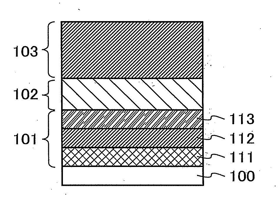
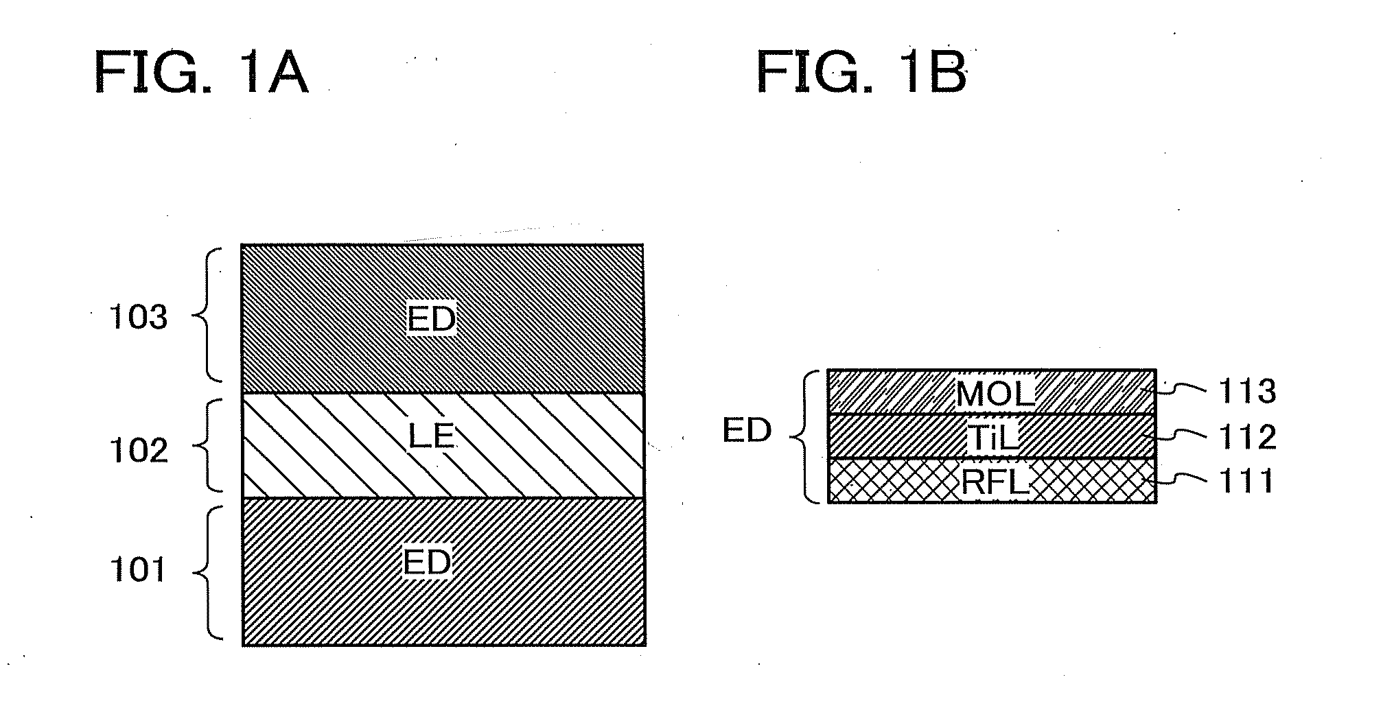
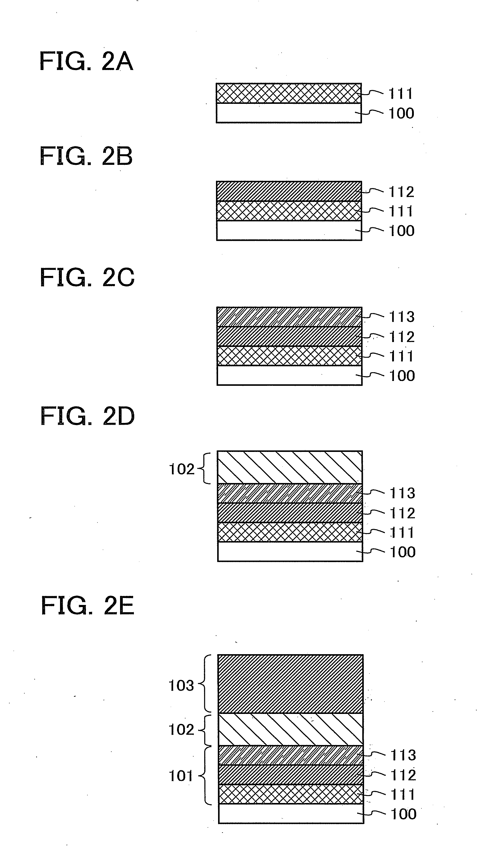
[0030]The light-emitting element includes, as shown in FIG. 1A, an electrode layer (also referred to as ED) 101, a light-emitting layer (also referred to as LE) 102, and an electrode layer 103.

[0031]Note that an electrode layer is a layer functioning as an electrode.

[0032]The electrode layer 101 functions as an electrode of the light-emitting element.

[0033]The light-emitting layer 102 emits light with a particular color by application of voltage. The light-emitting layer 102 includes M (M is a natural number) light-emitting units.

[0034]Voltage generally refers to a difference between potentials at two points (also referred to as a potential difference). However, values of both a ...

embodiment 2

[0066]In this embodiment, structural examples of a light-emitting layer (LE) of the light-emitting element in the above embodiment will be described.

[0067]The light-emitting layer includes M light-emitting units (also referred to as LEU).

[0068]The structural examples of the light-emitting unit in this embodiment will be described with reference to FIGS. 3A to 3D. FIGS. 3A to 3D are schematic cross-sectional views each illustrate the structural example of the light-emitting unit in this embodiment.

[0069]A light-emitting unit illustrated in FIG. 3A includes an electroluminescence layer (also referred to as ELL) 121a.

[0070]The electroluminescence layer 121a includes a light-emitting material.

[0071]A light-emitting unit illustrated in FIG. 3B includes the electroluminescence layer 121b, a hole-injection layer (also referred to as HIL) 122, a hole-transport layer (also referred to as HTL) 123, an electron-transport layer (also referred to as ETL) 124, and an electron-injection layer (al...

embodiment 3

[0145]In this embodiment, an example of a display device provided with the light-emitting element in the above embodiment in a pixel portion will be described.

[0146]First, an example of the display device in this embodiment will be described with reference to FIG. 4. FIG. 4 is a diagram for explaining the display device in this embodiment.

[0147]The display device illustrated in FIG. 4 includes a display driving portion DDRV and a pixel portion PIX.

[0148]The display driving portion DDRV controls display operation in the display device.

[0149]The pixel portion PIX performs the display operation.

[0150]The display device illustrated in FIG. 4 includes a driver circuit (also referred to as DRV) 301, a driver circuit 302, and a plurality of display circuits (also referred to as DISP) 305.

[0151]The driver circuit 301 is provided for or the display driving portion DDRV. The driver circuit 301 has a function of selecting the display circuit 305.

[0152]The driver circuit 301 has a shift registe...


PUM


Abstract

A light-emitting element disclosed includes a first electrode layer; a second electrode layer which transmits light; and a light-emitting layer interposed between the first electrode layer and the second electrode layer. The first electrode layer includes a first conductive layer which is able to reflect light, a second conductive layer provided over the first conductive layer and including titanium, and a third conductive layer which transmits light and contains a metal oxide having work function higher than that of a material of the first conductive layer.

Description

BACKGROUND OF THE INVENTION[0001]1. Field of the Invention[0002]The present invention relates to a light-emitting element. The present invention relates to a display device including the light-emitting element in a pixel portion. The present invention further relates to a lighting device including the light-emitting element in a light-emitting portion.[0003]2. Description of the Related Art[0004]In recent years, a light-emitting element which is one of the electro-optical elements and contains an organic compound or an inorganic compound which emits light by applying voltage or current (the light-emitting element is also referred to as an electroluminescent element or an EL element) has been developed.[0005]The light-emitting element includes at least a first electrode, a second electrode, and a light-emitting layer overlapping with the first electrode and the second electrode and emits light in accordance with voltage applied between the first electrode and the second electrode.[00...

Claims


Application Information

Patent Timeline
Patent Type & Authority Applications(United States)
IPC IPC(8): H01L33/48
CPCH01L51/5206H01L51/5036Y02E10/549H10K50/125H10K50/818H10K50/852H01L21/02186H10K10/488H10K30/151H10K50/81
Inventor SASAKI, TOSHIKISUGISAWA, NOZOMUIKEDA, HISAOSEO, SATOSHIOHSAWA, NOBUHARUYAMAZAKI, SHUNPEI
Owner SEMICON ENERGY LAB CO LTD
Why Eureka
Try Eureka