Nanoparticle

Pending Publication Date: 2022-09-22
MERCK PATENT GMBH
View PDF0 Cites 0 Cited by
  • Summary
  • Abstract
  • Description
  • Claims
  • Application Information

AI Technical Summary

Benefits of technology

[0010]However, the inventors newly have found that there is still one or more of considerable problems for which improvement is desired, as listed below; improvement of particle size distribution, better Full Width at Half Maximum (FWHM) value, improved self-absorption value, improvement of absorption per mg of nanoparticle(s), improvement of quantum yield of nanoparticle, well-controlled shell thickness, improved charge injection ability of nanoparticle, higher device efficiency, lowering trap emission of nanoparticle, optimizing a surface condition of shell part of nanoparticle, reducing lattice defects of a shell layer of nanoparticle, reducing / preventing formation of dangling bonds of shell layer, better thermal stability, better chemical stability, improved chemical stability in desired solvent(s), improved thermal stability in desired solvent(s), improved chemical stability in desired matrix(es), improved thermal stability in desired matrix(es), improved dispersion in matrixes, improved dispersion in solvents, improved hole injection ability into semiconducting light emitting nanoparticle, improved external quantum efficiency, optimizing fabrication process of nanoparticle, providing new fabrication process to improve size control of nanoparticle, providing new fabrication process for better kinetics control in shell formation, new shell formation process to realize well controlled shell thickness and / or reducing lattice defects of a shell layer, environmentally more friendly and safer fabrication process.

Problems solved by technology

However, the inventors newly have found that there is still one or more of considerable problems for which improvement is desired, as listed below; improvement of particle size distribution, better Full Width at Half Maximum (FWHM) value, improved self-absorption value, improvement of absorption per mg of nanoparticle(s), improvement of quantum yield of nanoparticle, well-controlled shell thickness, improved charge injection ability of nanoparticle, higher device efficiency, lowering trap emission of nanoparticle, optimizing a surface condition of shell part of nanoparticle, reducing lattice defects of a shell layer of nanoparticle, reducing / preventing formation of dangling bonds of shell layer, better thermal stability, better chemical stability, improved chemical stability in desired solvent(s), improved thermal stability in desired solvent(s), improved chemical stability in desired matrix(es), improved thermal stability in desired matrix(es), improved dispersion in matrixes, improved dispersion in solvents, improved hole injection ability into semiconducting light emitting nanoparticle, improved external quantum efficiency, optimizing fabrication process of nanoparticle, providing new fabrication process to improve size control of nanoparticle, providing new fabrication process for better kinetics control in shell formation, new shell formation process to realize well controlled shell thickness and / or reducing lattice defects of a shell layer, environmentally more friendly and safer fabrication process.

Method used


Image

  • Nanoparticle
  • Nanoparticle
  • Nanoparticle

Examples


working examples

Core Synthesis Example 1: Synthesis of Magic Sized Clusters (MSCs) Cluster Synthesis

[0428]In a 500 mL 4-neck flask, weight 4.65 g (15.9 mmol) of indium acetate and 13.25 g (58.0 mmol) of myristic acid. The flask is equipped with a reflux condenser, septa and a tap between the flask and the condenser.

[0429]Put under vacuum at 100° C. for 8 h 15 min to off-gas acetic acid under reduced pressure, and overnight at room T.

[0430]Day after, the solution heat again to 100° C. and evacuate for 1 hour and 45 min in those conditions.

[0431]Total evacuation time at 100° C. for 10 hours,

[0432]At pressure: 85 mtorr.

[0433]Fill the reaction flask with argon and add 100 mL of dry toluene. Heat the reaction to 110° C.

[0434]Inject the mixture of 2.33 mL (2.0 g) of PTMS and 50 mL (43.5 g) of toluene into the flask with indium myristate (In(Ma) at 110° C.

[0435]The formation of MSCs was monitored via UV—vis of timed aliquots taken from the reaction solution. There was a gradual improvement in the peak sha...

working example 1

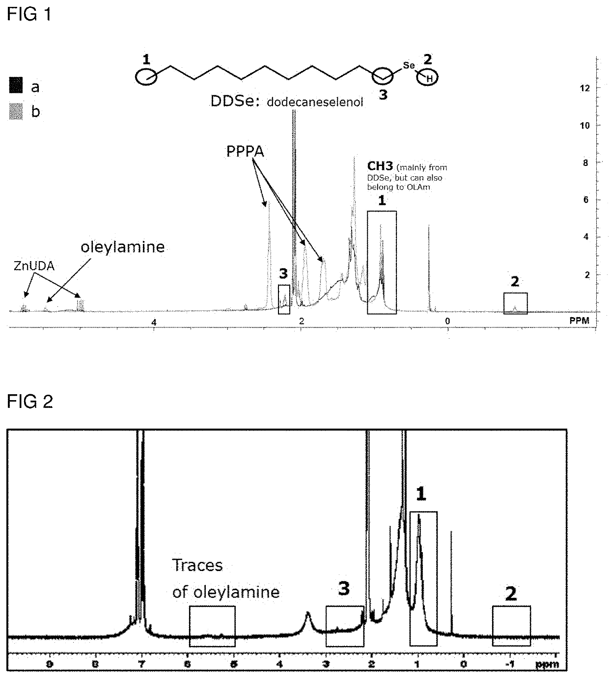
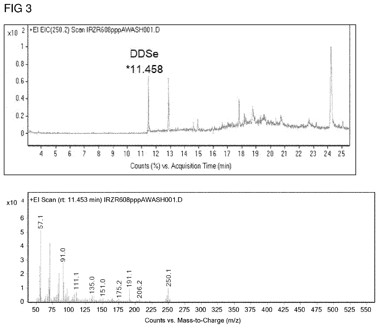
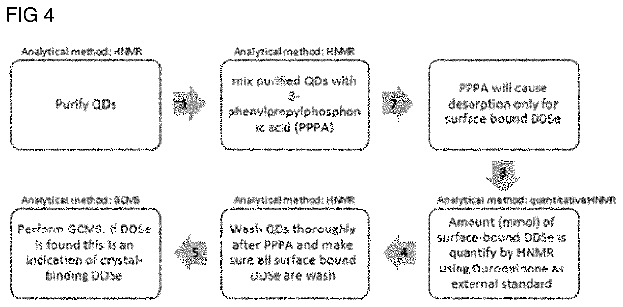
Synthesis on InP / ZnSe NPs in ODE, with 1-dodecaneselenol (DDSe) as Se Source

[0460]Outer layer synthesis: At room temperature, 8.3×10⁻⁸ mol of InP / ZnSe, described in comparative example 1, are dissolved with 0.2 ml toluene and transferred into 50 ml round bottom flask with 4 ml pumped 1-octadecene (ODE). After 30 min pumping at RT 1-dodecane selenol (0.2 mmol) is added and the flask is heated to 150° C. When temperature reached 150° C. Zn(Undecylenate)2 (0.2 mmol) is added and the reaction kept at 150° C. for 1.5 hrs. After 1.5 hours at 150° C. the reaction is terminated by cooling down the reaction mixture.

[0461]The resulting nanoparticles are is cleaned with a mixture of anhydrous toluene and ethanol (ratio crude:toluene:ethanol: 3:4:8). The process is repeated. Then the nanoparticles are extracted with hexane.

[0462]Table A compares the values of thermal, anti-radical, anti-peroxide stabilities for the described example and the comparative example 1.

working example 2

ynthesis on InP / ZnSe NPs in ODE, with 1-dodecanethiol as S Source

[0463]The working example is similar to working example 1, but 1-dodecanethiol is used as sulphur precursor.


PUM

PropertyMeasurementUnit
temperatureaaaaaaaaaa

Abstract

The present invention relates to a semiconducting nanoparticle; and a process for synthesizing the nanoparticle.

Description

FIELD OF THE INVENTION[0001]The present invention relates to a nanoparticle; a process for preparing a nanoparticle; composition, formulation and use of a nanoparticle, an optical medium; and an optical device.BACKGROUND ART[0002]Light emitting nanoparticles are known in the prior art documents.[0003]For example, Turo et al., ACS NANO vol. 8, no. 10, 10205-10203, 2014 discloses Cu2S Nanoparticles having no shell layers with dodecanethiol (DDT) and the fabrication process with using DDT at the temperature of 200° C. DDT was used in the entire synthesis process.[0004]Turo et al., Chem Commun, 2016, 52, 1 221 4-1 221 7 describes CdSe / ZnS with dodecanethiol.[0005]Robinson et al., Chem Mater, 2017, 29, 3854-3857 mentions quasi spherical Cu2S nanorods with DDT.PATENT LITERATURE[0006]No literatureNON-PATENT LITERATURE[0007]1. Turo et al., ACS NANO vol. 8, no. 10, 10205-10203, 2014[0008]2. Chem Commun, 2016, 52, 1 221 4-1 221 7[0009]3. Robinson et al., Chem Mater, 2017, 29, 3854-3857SUMMARY...

Claims


Application Information

Patent Timeline
Patent Type & Authority Applications(United States)
IPC IPC(8): C09K11/02C09K11/54C09K11/70C09K11/88B82Y40/00
CPCC09K11/025C09K11/54C09K11/70C09K11/883B82Y40/00
Inventor KOSSOY, ELIZAVETANEYSHTADT, SHANYKHALIL, SANAARABKIN, ALEXBENJAMINI ETTEDGUI, JESSICA
Owner MERCK PATENT GMBH
Why Eureka
Try Eureka