DNA sensor based on thin film transistor and preparation method thereof

A technology of thin-film transistors and sensors, applied in the field of DNA sensors, can solve the problems of reducing sensitivity, reducing the stability and repeatability of DNA sensors, etc., and achieve the goal of improving sensitivity, enhancing saturation current and carrier mobility, and eliminating the labeling process Effect

Pending Publication Date: 2021-05-28
SHANGHAI INSTITUTE OF TECHNOLOGY
View PDF0 Cites 0 Cited by
  • Summary
  • Abstract
  • Description
  • Claims
  • Application Information

AI Technical Summary

Problems solved by technology

However, most of them are based on the physical absorption of DNA molecules on the semiconductor and are realized by changing the electrical characteristics of the transistor, but the physical absorption based on the semiconductor will be sensitive to moisture and some ions, which will reduce the stability and stability of the DNA sensor. repeatability, thereby reducing its sensitivity

Method used


Image

  • DNA sensor based on thin film transistor and preparation method thereof
  • DNA sensor based on thin film transistor and preparation method thereof
  • DNA sensor based on thin film transistor and preparation method thereof

Examples


Embodiment 1

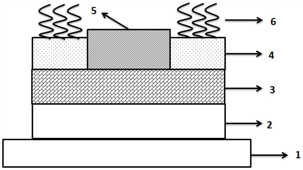
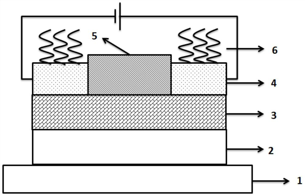
[0038] The structure of a thin-film transistor-based DNA sensor such as figure 1 As shown, the DNA sensor is composed of a recognition element and a transducer, and the DNA molecular probe 6 is used as the recognition element, and the DNA molecular probe 6 is solidified on the surface of the source-drain electrode 4 by means of adsorption, bonding, self-assembly, etc.; The transducer uses a thin film transistor, and the function of the transducer is to convert the signal sensed by the identification element into other recordable signals, such as mass change, frequency change, magnetic signal, fluorescent signal, electrical signal and acoustic wave signal. The DNA sensor is sequentially connected by the substrate substrate 1, the gate electrode 2, and the insulating layer 3, and then the source-drain electrode 4 is prepared on the insulating layer 3, and the DNA molecular probe 6 is fixed on the source-drain electrode 4, and finally the source-drain electrode 4 A semiconductor ...

Embodiment 2

[0050] The structure of the DNA sensor in this embodiment is basically the same as in Embodiment 1, the difference is that:

[0051] In this example, see Figure 5 , which is sequentially connected by the substrate substrate 1, the gate electrode 2, the insulating layer 3, and the semiconductor layer 5, and then the source-drain electrode 4 is made on the semiconductor layer 5 to form a bottom-gate-top contact structure, and finally on the source-drain electrode 4 Immobilized DNA molecular probes.

[0052] The specific preparation method of each structural layer of the thin film transistor in this embodiment is as follows:

[0053] 1) Select a heavily doped silicon wafer as the substrate 1 and the gate electrode 2. The conductivity of the silicon wafer is 0.01-0.15 Ω·cm, and the substrate 1 is ultrasonically cleaned with acetone and ethanol for fifteen minutes; Rinse with the corresponding solvent when taking it out to remove the adhered debris;

[0054] 2) Thermally oxidiz...

Embodiment 3

[0067] A DNA sensor based on a thin film transistor, the DNA sensor includes a thin film transistor and a DNA molecular probe 6, the thin film transistor includes a substrate substrate 1, a gate electrode 2, an insulating layer 3, source and drain electrodes 4 and a semiconductor layer 5, the substrate substrate 1. The gate electrode 2 and the insulating layer 3 are arranged sequentially from bottom to top, the semiconductor layer 5 is arranged on the insulating layer 3 , the source and drain electrodes 4 are in contact with the semiconductor layer 5 , and the DNA molecular probe 6 is fixed on the source and drain electrodes 4 .

[0068] Wherein, both the source and drain electrodes 4 and the semiconductor layer 5 are disposed on the insulating layer 3 , and the semiconductor layer 5 is located in the channel of the source and drain electrodes 4 .

[0069] Substrate The material of the substrate 1 is an insulating material, or a composite material formed by covering the surface...


PUM


Abstract

The invention relates to a DNA sensor based on a thin film transistor and a preparation method thereof.The DNA sensor comprises the thin film transistor and a DNA molecular probe, the thin film transistor comprises a substrate, a gate electrode, an insulating layer, source and drain electrodes and a semiconductor layer, the substrate, the gate electrode and the insulating layer are sequentially arranged from bottom to top, the semiconductor layer is arranged on the insulating layer, and the source and drain electrodes are in contact with the semiconductor layer, and the DNA molecular probe is fixed on the source and drain electrodes. Compared with the prior art, the source and drain electrodes are used as the substrate, and the DNA molecular probes are fixed on the source and drain electrodes, so that the influence of physical absorption on the organic semiconductor layer on moisture and certain ions is avoided, charge injection is improved, the saturation current and carrier mobility of the sensor are enhanced, and the stability and sensitivity of the DNA sensor are improved.

Description

technical field [0001] The invention belongs to the technical field of DNA sensors, and relates to a thin-film transistor-based DNA sensor and a preparation method thereof. Background technique [0002] With the development of technologies such as bioinformatics and the Internet of Things, DNA molecules, as the most basic substance in bioengineering, have attracted the attention of a large number of scientific research institutes, and the development of DNA detection technology has also promoted the continuous advancement of research on DNA structure and function. . At present, DNA detection technologies include traditional DNA sequencing technology, DNA chips, biosensors, etc. Among them, DNA biosensor has the characteristics of fast detection speed and high sensitivity, and has been widely used in environmental monitoring, aerospace and other fields. [0003] In recent years, the research and application of organic transistor devices have been greatly developed, and DNA ...

Claims


Application Information

Patent Timeline
IPC IPC(8): H01L29/786H01L29/417H01L21/336H01L21/34G01N27/327
CPCH01L29/786H01L29/78684H01L29/7869H01L29/41733H01L29/66045H01L29/66969H01L29/66742G01N27/327
Inventor 王军陈赛赛毛毓珂王桂东蔡金华
Owner SHANGHAI INSTITUTE OF TECHNOLOGY
Why Eureka
Try Eureka