

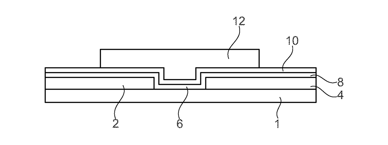
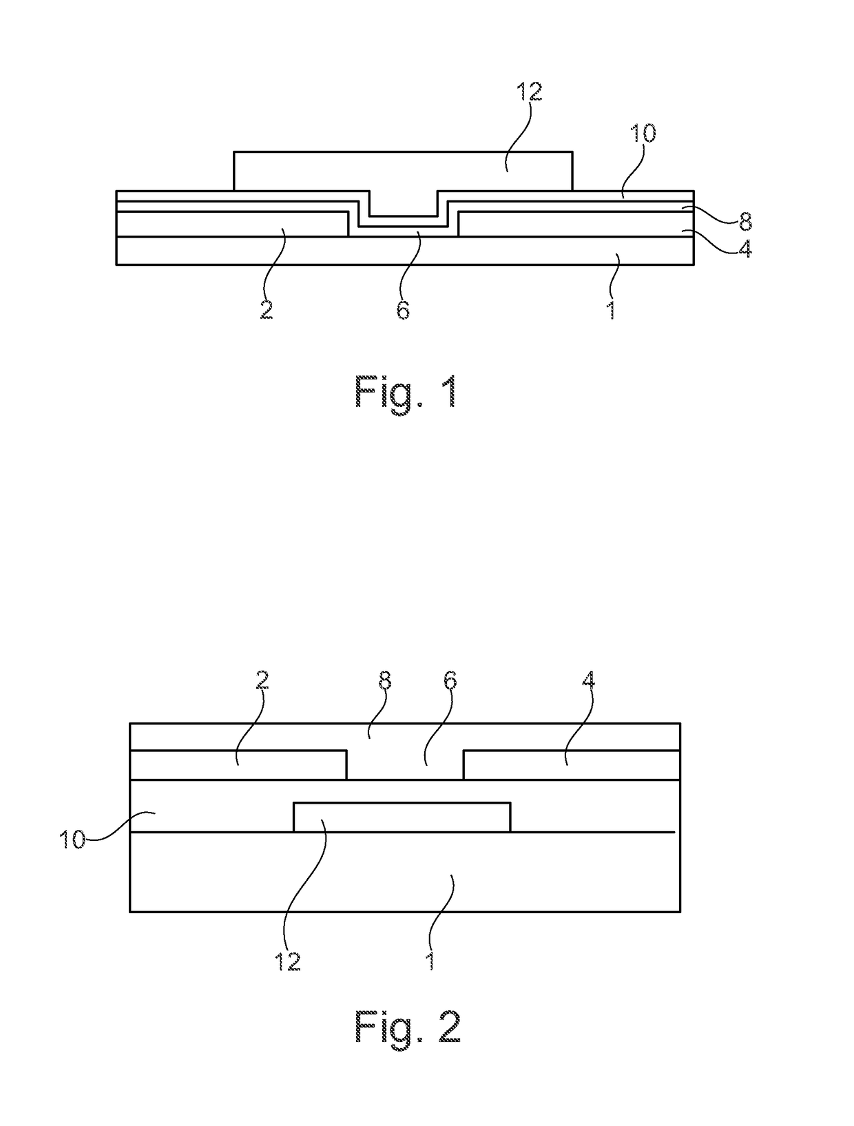
Electrode surface modification layer for electronic devices
a technology of electronic devices and surface modification layers, applied in semiconductor devices, solid-state devices, electrical apparatuses, etc., can solve the problems of low device mobility, and achieve the effect of improving matching, increasing work functions, and increasing work efficiency
- Summary
- Abstract
- Description
- Claims
- Application Information
AI Technical Summary
Benefits of technology
Problems solved by technology
Method used
Image

Examples
examples
Materials
[0187]Toluene and o-xylene was obtained from Sigma-Aldrich.[0188]Mo(tfd)3 (shown below) was prepared by the method described in as described in Inorganic Syntheses, Volume 10, Part 1, Chapter 1, p 8-26 “Metal complexes derived from cis-1,2-dicyano-1,2-ethylenedithiolate and bis(trifluoromethyl)-1,2-dithiete”, by A. Davison, R. H. Holm, R. E. Benson and W. Mahler.
[0189][0190]The substrate is glass obtained from Corning.[0191]Gold is obtained from agar scientific 99.99%.[0192]The organic semiconducting layer is described below.[0193]The gate dielectric is PTFE. A commercially available PTFE is used.[0194]Aluminium is obtained from Agar scientific 99.999%.
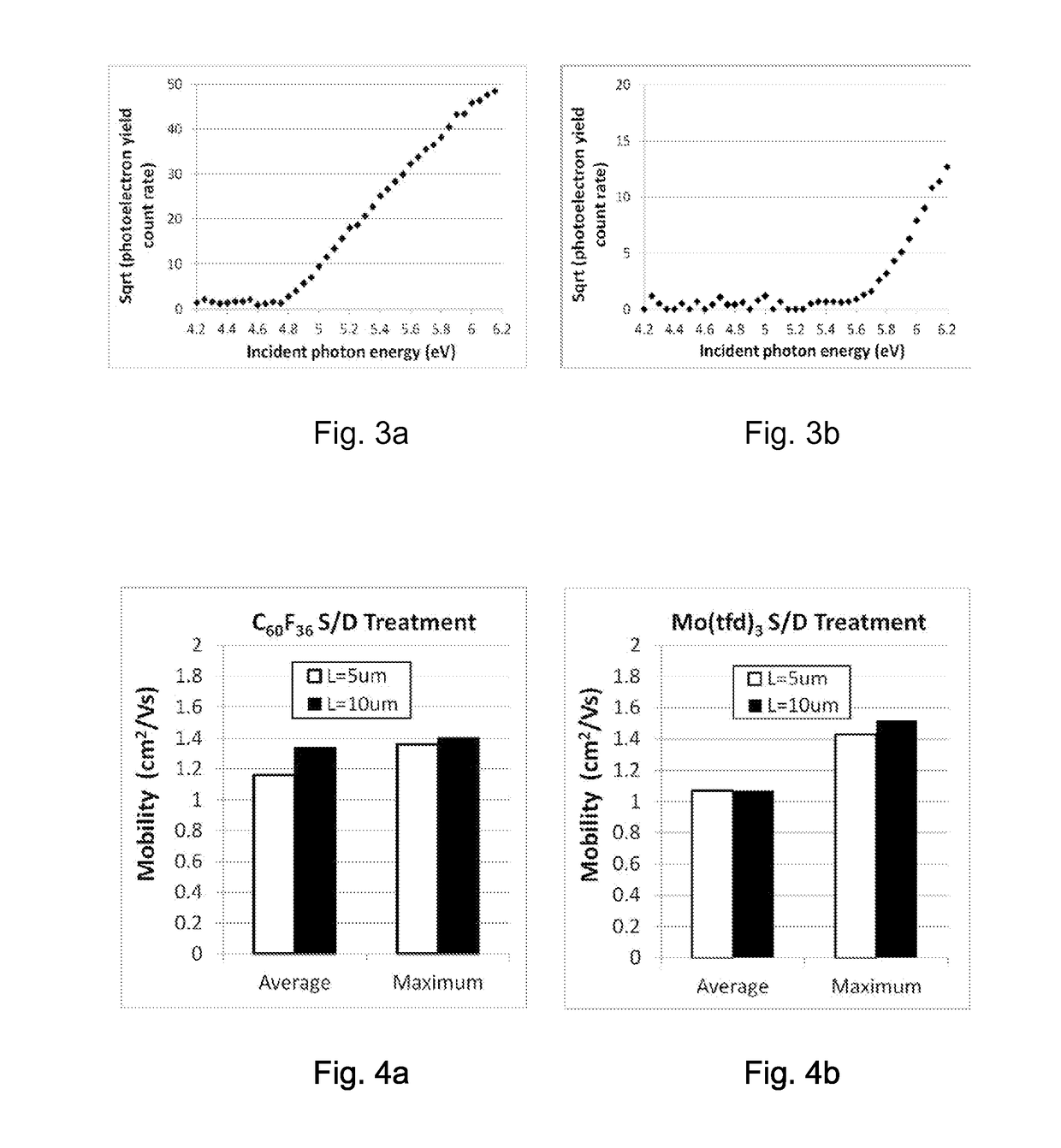
Determination of Work Function of Modified Electrodes
[0195]Samples were prepared by thermally evaporating gold (40 nm) onto a glass substrate. The substrates were immersed in a solution of Mo(tfd)3 in toluene (1 mg / ml) for 5 minutes and then rinsed with toluene to remove any non-absorbed complex from the substrate and dried a...
PUM
| Property | Measurement | Unit |
|---|---|---|
| LUMO | aaaaa | aaaaa |
| polydispersity | aaaaa | aaaaa |
| thickness | aaaaa | aaaaa |
Abstract
Description
Claims
Application Information