

Magnetic random access memory
a random access and memory technology, applied in the field of magnetic random access memory, can solve the problems of low signal ratio (mr ratio) and commercialization problems
- Summary
- Abstract
- Description
- Claims
- Application Information
AI Technical Summary
Problems solved by technology
Method used
Image

Examples
first embodiment
[2] First Embodiment
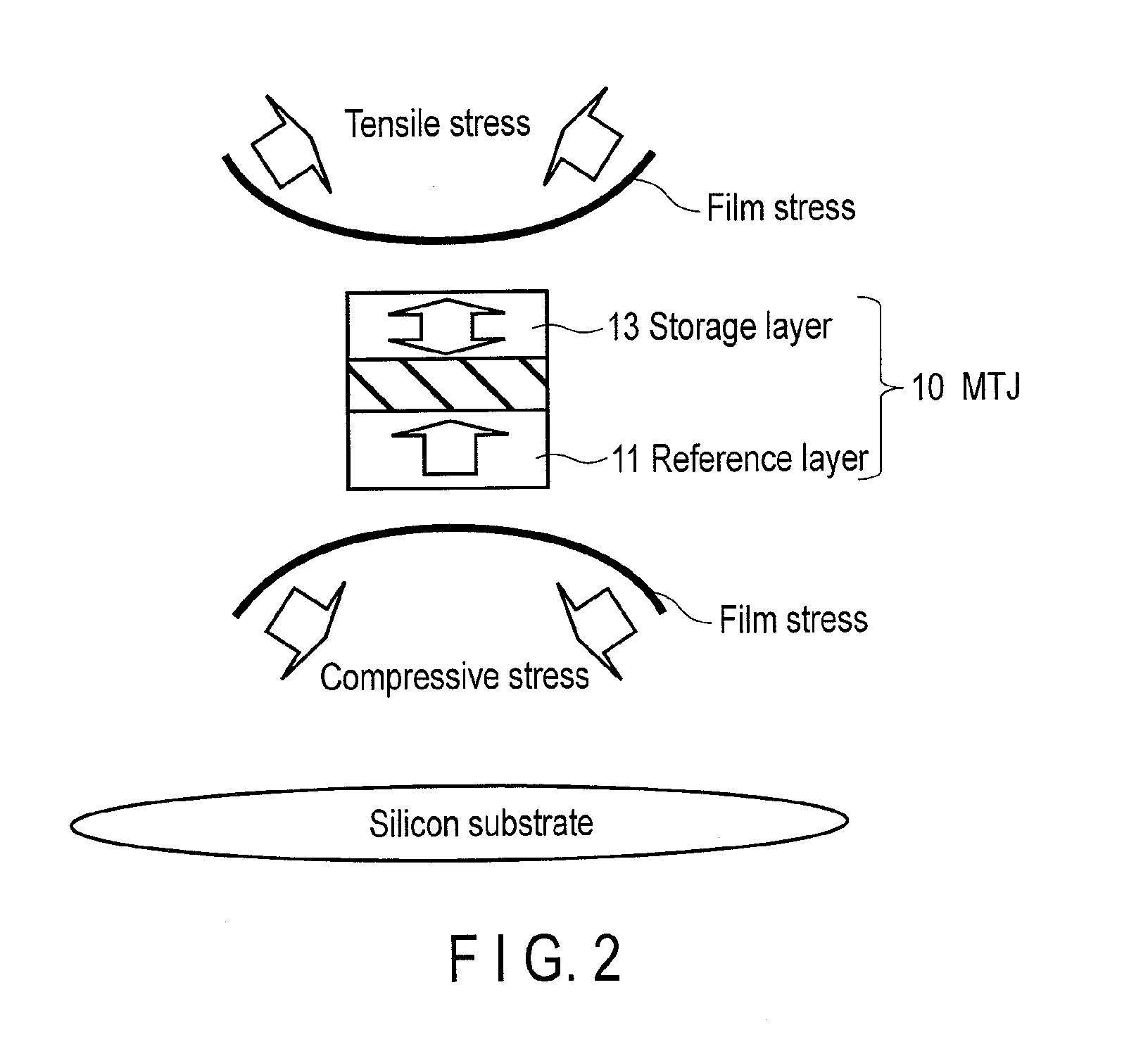
[0029]In the first embodiment, a stress film having a tensile stress with respect to a semiconductor substrate is arranged on the upper side of an MTJ element 10.
[0030]The structure around the MTJ element 10 according to the first embodiment will be described with reference to FIG. 3.
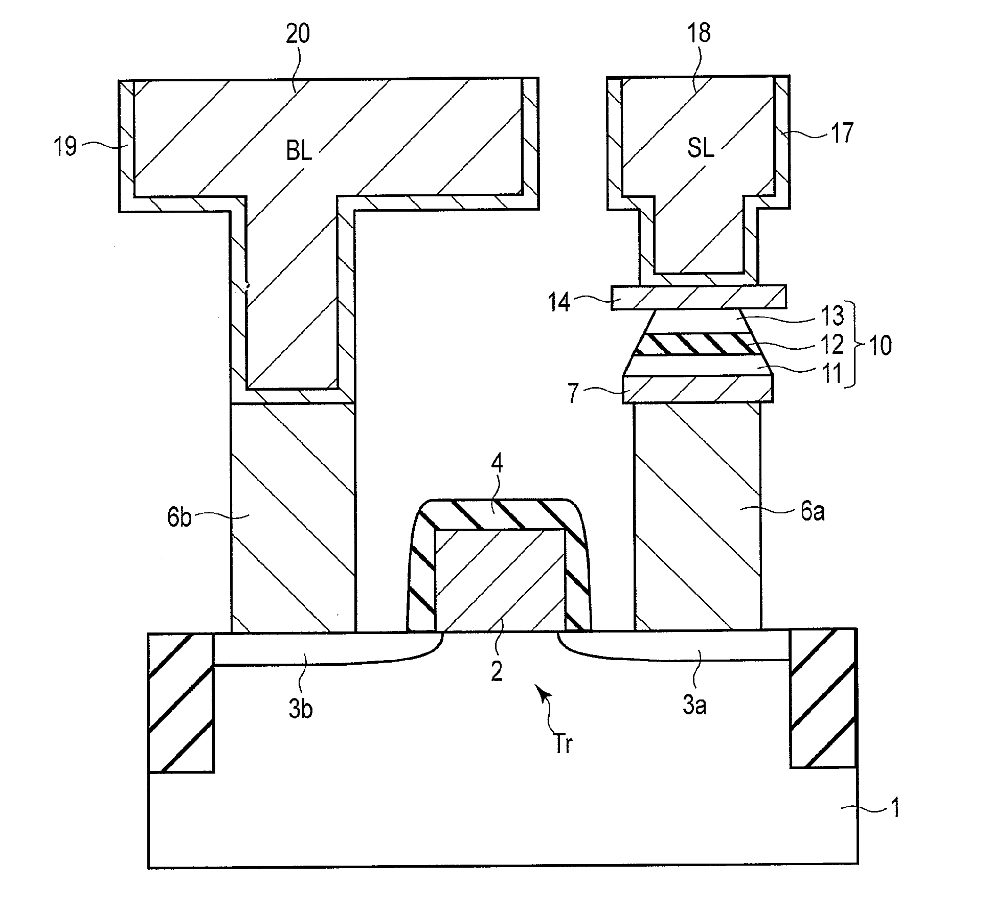
[0031]As shown in FIG. 3, a lower electrode 7 connected to a contact 6a is formed on the contact 6a and an interlayer insulation film 5. The MTJ element 10 is formed on the lower electrode 7. An upper electrode 14 is formed on the MTJ element 10. The upper electrode 14 may be the hard mask used when processing the MTJ element 10. The planar shape of the upper electrode 14 can be the same as that of the MTJ element 10. The side surfaces of the upper electrode 14 can match those of the MTJ element 10. A sidewall insulating film 15 is formed on the side surfaces of the MTJ element 10 and the upper electrode 14. The outer edge of the button surface of the sidewall insulating film 15 matc...
second embodiment
[3] Second Embodiment
[0038]In the second embodiment, a stress film having a compressive stress with respect to a semiconductor substrate is arranged on the lower side of an MTJ element 10. In the second embodiment, points different from the first embodiment will mainly be explained.
[0039]The structure around the MTJ element 10 according to the second embodiment will be described with reference to FIG. 5.
[0040]As shown in FIG. 5, the second embodiment is different from the first embodiment in that a silicon nitride film 22 functioning as a compressive stress film is arranged on the lower side of the MTJ element 10.
[0041]The silicon nitride film 22 is formed on an interlayer insulation film 5 around a lower electrode 7. The silicon nitride film 22 can have a film thickness equal to or different from that of the lower electrode 7. To make the silicon nitride film 22 function as the compressive stress film, SiN preferably has an SiN density of 3 g / cm3 or less and an N—H amount of 5×10²¹...
third embodiment
[4] Third Embodiment
[0046]In the third embodiment, a stress film having a tensile stress with respect to a semiconductor substrate is arranged on the side surfaces of an upper electrode 14 located on the upper side of an MTJ element 10. In the third embodiment, points different from the first embodiment will mainly be explained.
[0047]The structure around the MTJ element 10 according to the third embodiment will be described with reference to FIG. 7.
[0048]As shown in FIG. 7, the third embodiment is different from the first embodiment in that a silicon nitride film 24 functioning as a stress film is arranged on an oxide film 23 on the side surfaces of the MTJ element 10 and the upper electrode 14.
[0049]The silicon nitride film 24 is formed on a portion corresponding to the upper portion of the MTJ element 10 (that is, on the side surfaces of the upper electrode 14), and functions as a tensile stress film. That is, SiN of the silicon nitride film 24 preferably has an SiN density of 3 g...
PUM
 Abstract
Description
Claims
Application Information