Optical waveguide substrate and method for manufacturing same

a technology of optical waveguides and substrates, applied in the direction of optical elements, manufacturing tools, instruments, etc., can solve the problems of patent documents 1 and 2 failing to provide detailed descriptions, and the speed and density increase of electrical wiring in the related art is approaching the limit, so as to achieve a small transmission loss of light and high degree of accuracy

Inactive Publication Date: 2012-08-30
HITACHI CHEM CO LTD
View PDF6 Cites 20 Cited by
  • Summary
  • Abstract
  • Description
  • Claims
  • Application Information

AI Technical Summary

Benefits of technology

[0016]According to the method of the present invention, it becomes possible to provide an optical waveguide substrate in which an optical axis conversion mirror in the optical waveguide substrate and a light receiving and emitting element are aligned with respect to each other at so extremely high a degree of accuracy that a transmission loss of light is small and a manufacturing method thereof, and further an opto-electric hybrid board obtained by combining the optical waveguide and electrical wiring and a manufacturing method thereof as well as an alignment recess forming apparatus for an optical waveguide substrate. More specifically, it becomes possible to manufacture an opto-electric hybrid board in which an amount of relative positional misalignment of the optical waveguide with respect to the light receiving and emitting element is within ±10 μm.

Problems solved by technology

With high-speed and high-density signal transmissions between electronic elements or between circuit boards in recent years, an increase in speed and density by transmissions via electrical wiring in the related art is approaching the limit because of an obstacle, such as mutual interference and attenuation of signals.
Patent Documents 1 and 2, however, fail to provide detailed descriptions as to in which manner the alignment marker and the alignment hole are obtained with accuracy.

Method used


Image

  • Optical waveguide substrate and method for manufacturing same
  • Optical waveguide substrate and method for manufacturing same
  • Optical waveguide substrate and method for manufacturing same

Examples


example 1

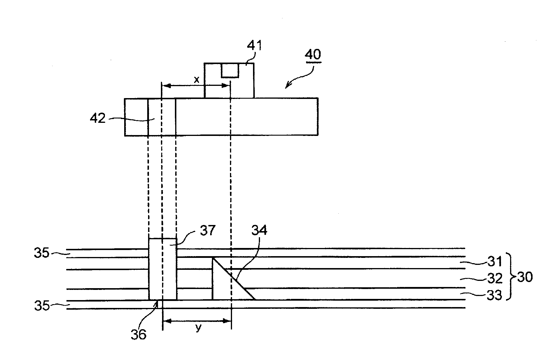
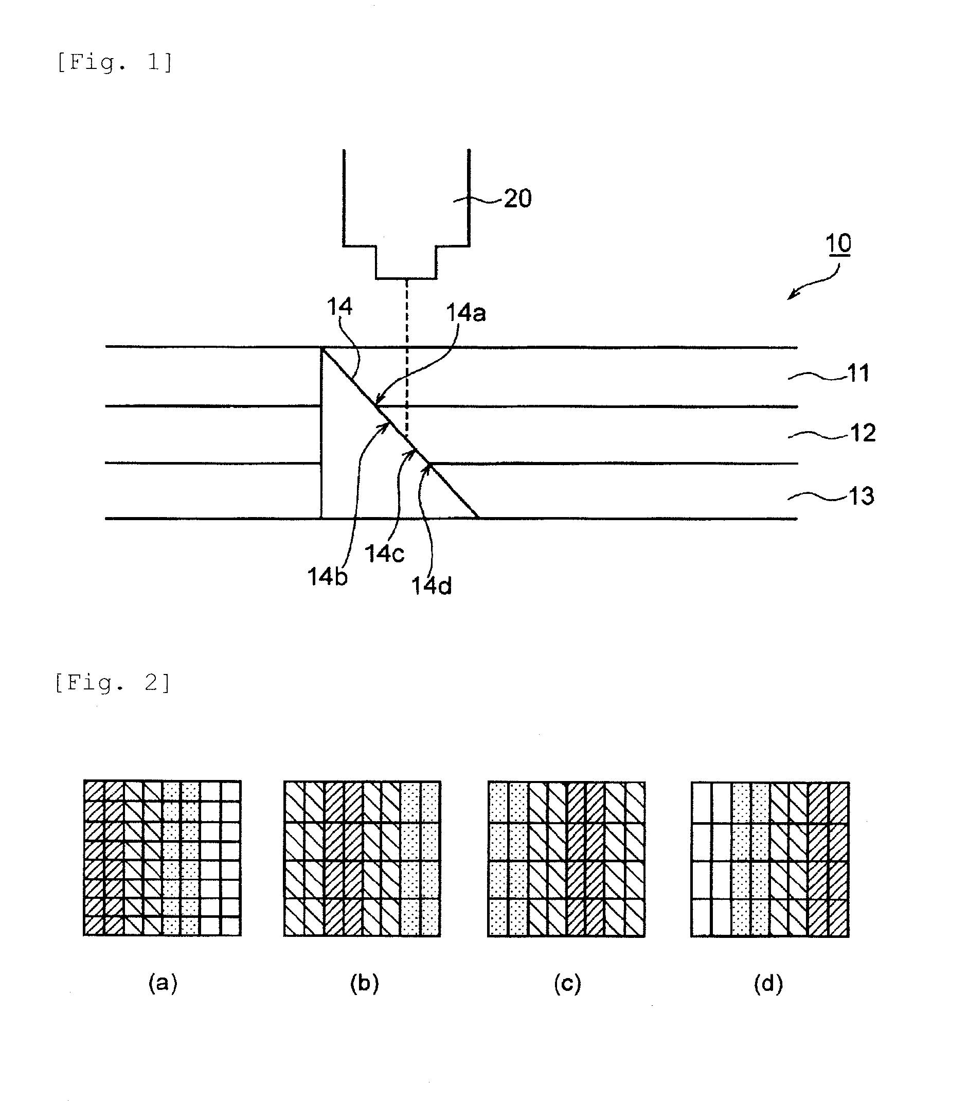
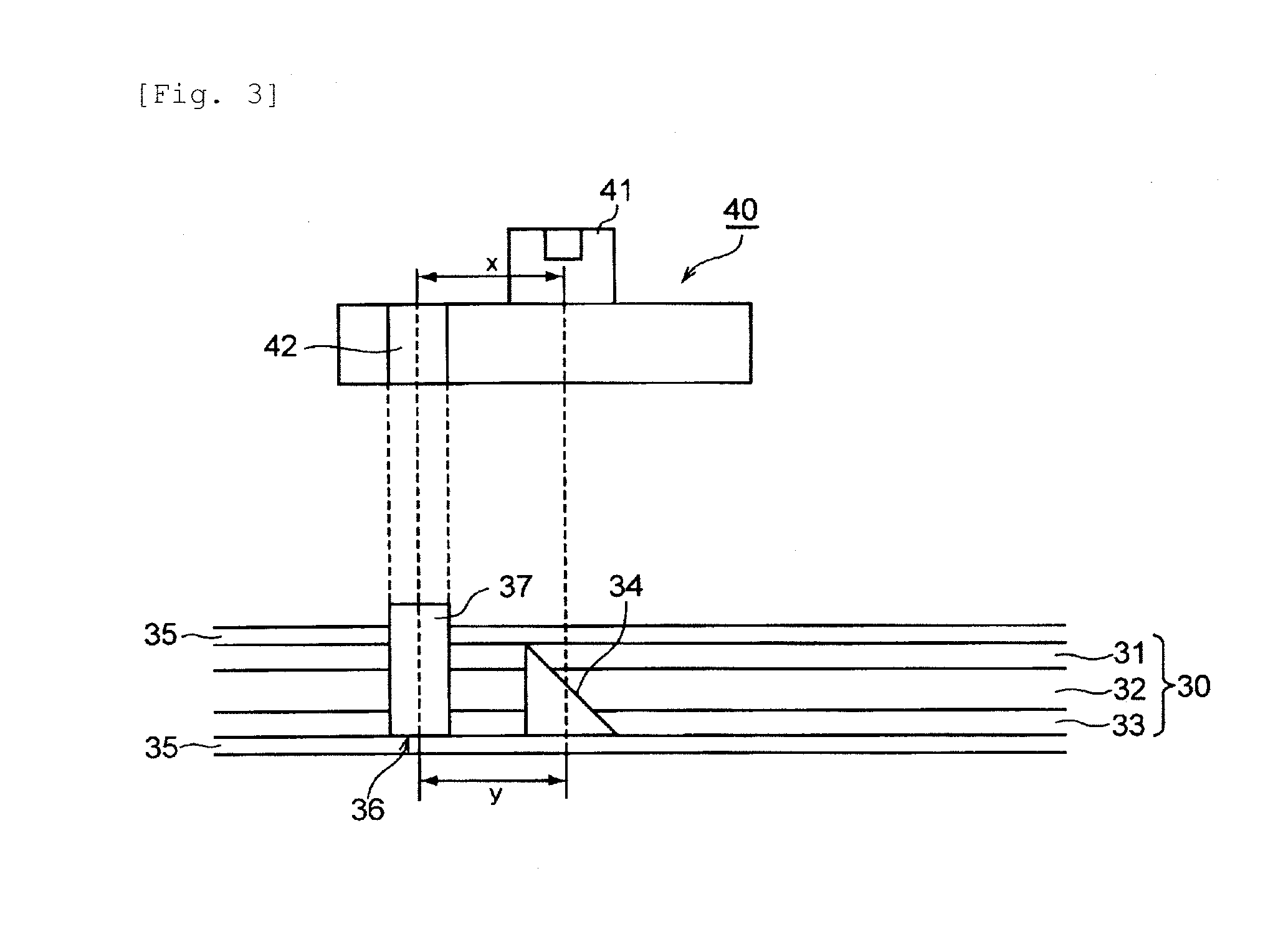
(1-1) Manufacturing of Optical Waveguide Film Manufacturing of Clad Layer Forming Resin Film

[0084]Herein, 48 parts by mass of phenoxy resin (available from Tohto Kasei Co., Ltd under the product name of PhenoTohto® YP-70) as the binder polymer (A), 49.6 parts by mass of alicyclic diepoxy carboxylate (available from Asahi Denka Kogyo K.K. under the product name of KRM-2110, molar weight: 252) as the photopolymerizable compound (B), 2 parts by mass of triphenyl sulfonium hexafluoro antimonate salt (available from Asahi Denka Kogyo K.K. under the product name of SP-170) as the photopolymerization initiator (C), 0.4 part by mass of SP-100 (available from Asahi Denka Kogyo K.K. under this product name) as an intensifier, and 40 parts by mass of propylene glycol monomethyl ether acetate as an organic solvent were weighted in a wide-mouth polyethylene bottle. The mixture was kept stirred for six hours with a mechanical stirrer, a shaft, and a propeller under conditions at a temperature of ...


PUM

PropertyMeasurementUnit
angleaaaaaaaaaa
distanceaaaaaaaaaa
mass %aaaaaaaaaa

Abstract

According to a manufacturing method of an optical waveguide substrate including a core (12) and clads (11) (13) and provided with an optical axis conversion mirror (14) in the core and an alignment recess for the optical axis conversion mirror with respect to a light receiving and emitting element, the recess is obtained by obtaining an outline of the core by synthesizing at least an image captured by focusing a microscope (20) to a highest position (14a) of the core in an optical axis conversion mirror portion and an image captured by focusing the microscope to a lowest position (14d), and by determining a position of the alignment recess in reference to a center of gravity of the outline, and according to an optical waveguide substrate obtained by this manufacturing method, it becomes possible to provide an optical waveguide substrate in which the optical axis conversion mirror in the optical waveguide substrate and the light receiving and emitting element are aligned with respect to each other at an extremely high degree of accuracy and a manufacturing method thereof.

Description

TECHNICAL FIELD[0001]The present invention relates to an optical waveguide substrate and a manufacturing method thereof, and more particularly, to an optical waveguide substrate in which an optical axis conversion mirror in the optical waveguide substrate and a light receiving and emitting element are aligned with respect to each other with accuracy and a manufacturing method thereof. Also, the present invention relates to an opto-electric hybrid board obtained by combining the optical waveguide and electrical wiring and a manufacturing method thereof and to an alignment recess forming apparatus for an optical waveguide substrate.BACKGROUND ART[0002]With high-speed and high-density signal transmissions between electronic elements or between circuit boards in recent years, an increase in speed and density by transmissions via electrical wiring in the related art is approaching the limit because of an obstacle, such as mutual interference and attenuation of signals. In order to overco...

Claims


Application Information

Patent Timeline
Patent Type & Authority Applications(United States)
IPC IPC(8): G02B6/12B23P19/00B23Q17/00
CPCY10T408/50H05K1/0274G02B6/122Y10T29/49764G02B6/4214G02B6/42
Inventor KURODA, TOSHIHIROSAKAI, DAICHIYAGI, SHIGEYUKISHIBATA, TOMOAKI
Owner HITACHI CHEM CO LTD
Why Eureka
Try Eureka