Organic electroluminescent devices

a technology of electroluminescent devices and organic materials, which is applied in the direction of thermoelectric device junction materials, semiconductor devices, electrical apparatus, etc., can solve the problems of inoperable devices, and achieve the effect of reducing failure ratio and manufacturing with less effor

Active Publication Date: 2012-09-13
BEIJING XIAOMI MOBILE SOFTWARE CO LTD
View PDF2 Cites 2 Cited by
  • Summary
  • Abstract
  • Description
  • Claims
  • Application Information

AI Technical Summary

Benefits of technology

[0003]It is an object of the present invention to provide a reliable organic electroluminescent device, which could be manufactured with less manufacturing effort and a method to manufacture such a device with a reduced failure ratio.

Problems solved by technology

Without any additional measure, such a device would not be operational, since both electrodes are electrically connected.

Method used


Image

  • Organic electroluminescent devices
  • Organic electroluminescent devices
  • Organic electroluminescent devices

Examples


Embodiment Construction

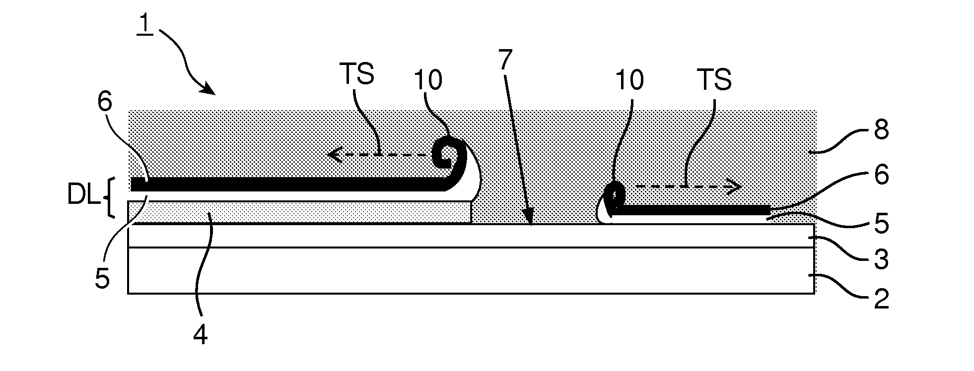
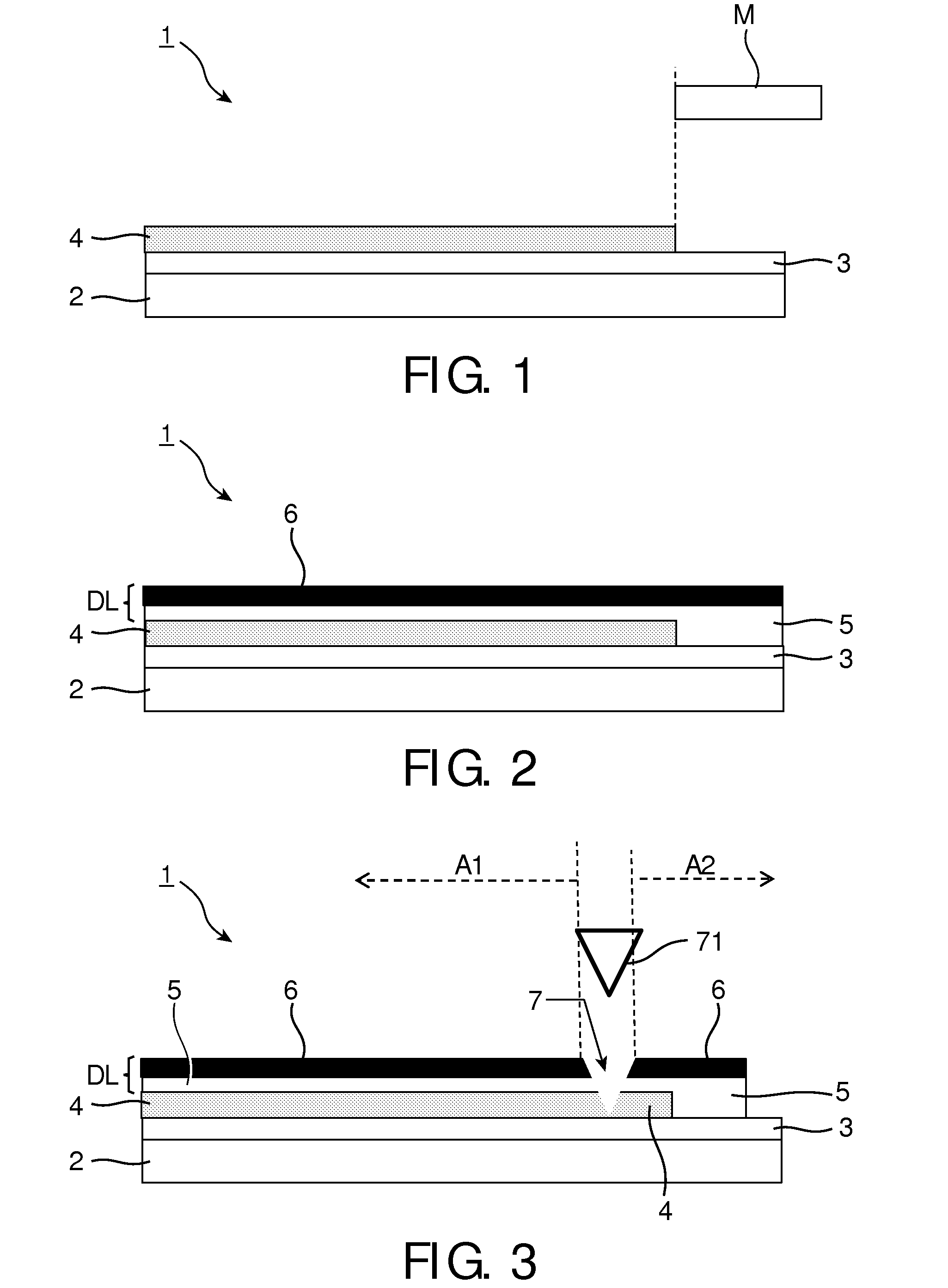
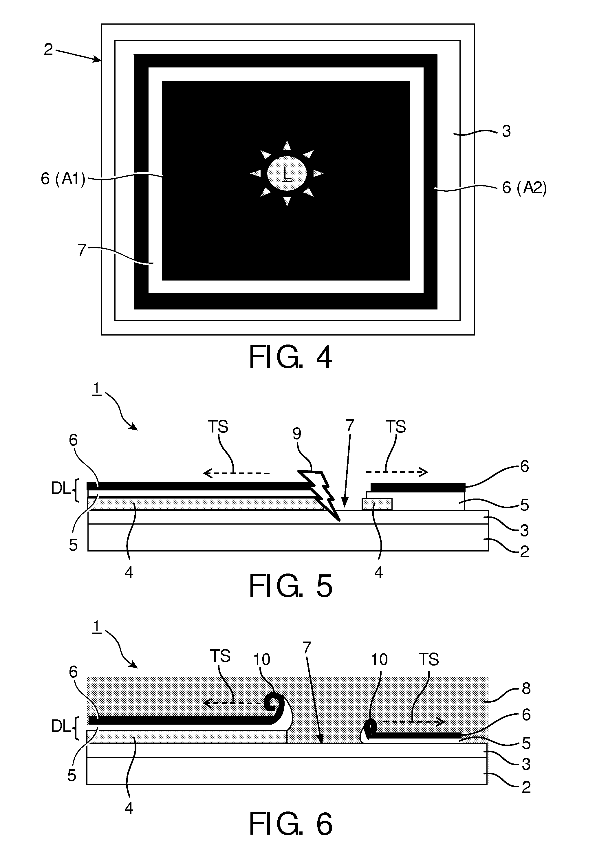
[0057]FIG. 1 is a schematic cross-sectional view of an organic electroluminescent (OLED) device after deposition of the electroluminescent layer stack. At this state of production the OLED device comprises for example a flat glass substrate 2 onto which a transparent ITO anode of a layer thickness of 120 nm as the substrate electrode 3 has been deposited by sputtering or CVD. On top of the substrate electrode 3 an organic electroluminescent layer stack 4 to emit light is deposited by vacuum evaporation comprising a 25 nm thick hole injection layer of NHT-5 α-NPD doped with 4% F4-TCNQ, a 10 nm thick hole transport layer of α-NPD, a 30 nm thick organic light emitting layer of a matrix material with embedded light emitting small molecules, and a 50 nm thick electron transporting layer of TPBI. People skilled in the art may chose alternative electroluminescent layer stack with additional layers or with a lower number of layer or even with a single organic light emitting layer within the...


PUM


Abstract

This invention relates to an organic electroluminescent device (1) produced with less effort comprising a substrate (2), a substrate electrode (3) on top of the substrate (2), an electroluminescent layer stack (4) with at least one organic light emitting layer on top of the substrate electrode (3), a counter electrode (5) at least covering the electroluminescent layer stack (4), and a short prevention layer (6) covering the counter electrode (5) establishing a double layer (DL) of counter electrode (5) and short prevention layer (6), and an electrically isolating layer at least partly on top of the short prevention layer, where a tensile stress (TS) is induced to the double layer (DL) by the short prevention layer (5) suitable to roll-up (10) the double layer (DL) after deposition of the electrically isolating layer (8) adjacent to a cut introduced at least to the double layer (DL) in an area, where the double layer (DL) is arranged on top of the electroluminescent layer stack (4) suitable to electrically disconnect the counter electrode (5) from the substrate electrode (3), where the electrically isolating layer (8) at least partly covers the area of the double layer with introduced cut (7) to partly dissolve the electroluminescent layer stack (4) to weaken the adhesion of the double layer to the electroluminescent layer stack adjacent to the cut to roll-up the double layer in the vicinity of the cut. The invention further relates to a method of manufacturing such an OLED device.

Description

FIELD OF THE INVENTION[0001]The invention relates to an OLED devices produced with less effort and to a method of manufacturing such an OLED devices.BACKGROUND OF THE INVENTION[0002]Organic electroluminescent devices (OLEDs) comprise very thin layers of organic substances on top of a glass substrate covered with an electrically conducting but optically transparent oxide, usually Indium-Tin oxide (ITO). ITO forms the substrate electrode, usually the anode and a layer of Aluminum (100 nm) evaporated on top of the organic layer stack forms the counter electrode, usually the cathode. When a voltage between 2 and typically 5 V is applied between the electrodes, current is injected into the organic layers and light is generated. The preparation of OLEDs requires structuring of all individual layers to provide a reliable operation over time, in particular to operate the OLEDs, both electrodes have to be electrically isolated from each other. Therefore at least three masks processes are com...

Claims


Application Information

Patent Timeline
Patent Type & Authority Applications(United States)
IPC IPC(8): H01L51/52H01L51/56
CPCH01L51/52H01L51/56H01L51/5203H10K50/80H10K50/805H10K71/00H10K50/11H10K50/13H10K50/8423
Inventor BOERNER, HERBERT F.
Owner BEIJING XIAOMI MOBILE SOFTWARE CO LTD
Why Eureka
Try Eureka