Semiconductor package structure and manufacturing method thereof

a technology of semiconductors and packaging, applied in the direction of semiconductor devices, semiconductor/solid-state device details, electrical apparatus, etc., can solve the problems of troublesome heat emission from light emitting diodes, shortening the service life reducing the brightness of light emitting diodes, so as to achieve better heat dissipation efficiency

Inactive Publication Date: 2012-09-13
UNISTARS
View PDF3 Cites 3 Cited by
  • Summary
  • Abstract
  • Description
  • Claims
  • Application Information

AI Technical Summary

Benefits of technology

[0026]Because the heat emitted from the semiconductor die can be dissipated to the outside environment via the thermall

Problems solved by technology

However, with the increasing brightness, the larger amount of heat emission from the light emitting diode has become a troublesome issue in the industry.
If the heat emission cannot be removed efficiently, the brightness of the light emitting diode will be decreased and the c

Method used


Image

  • Semiconductor package structure and manufacturing method thereof
  • Semiconductor package structure and manufacturing method thereof
  • Semiconductor package structure and manufacturing method thereof

Examples


first embodiment

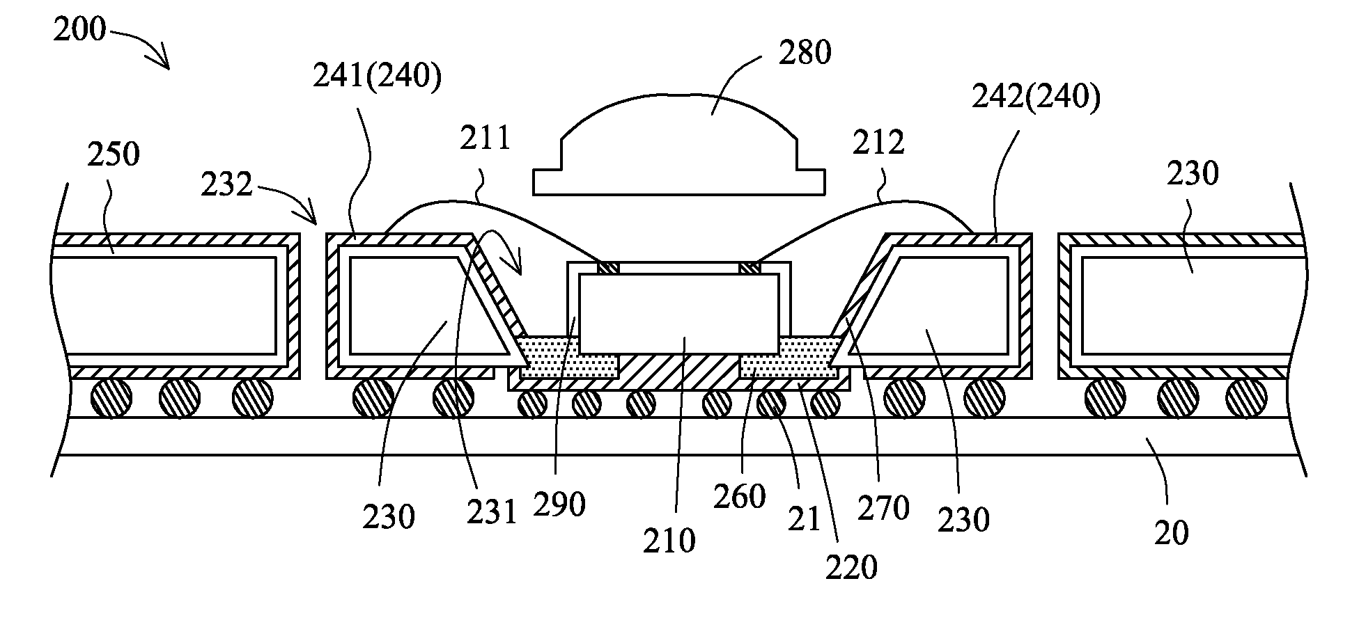
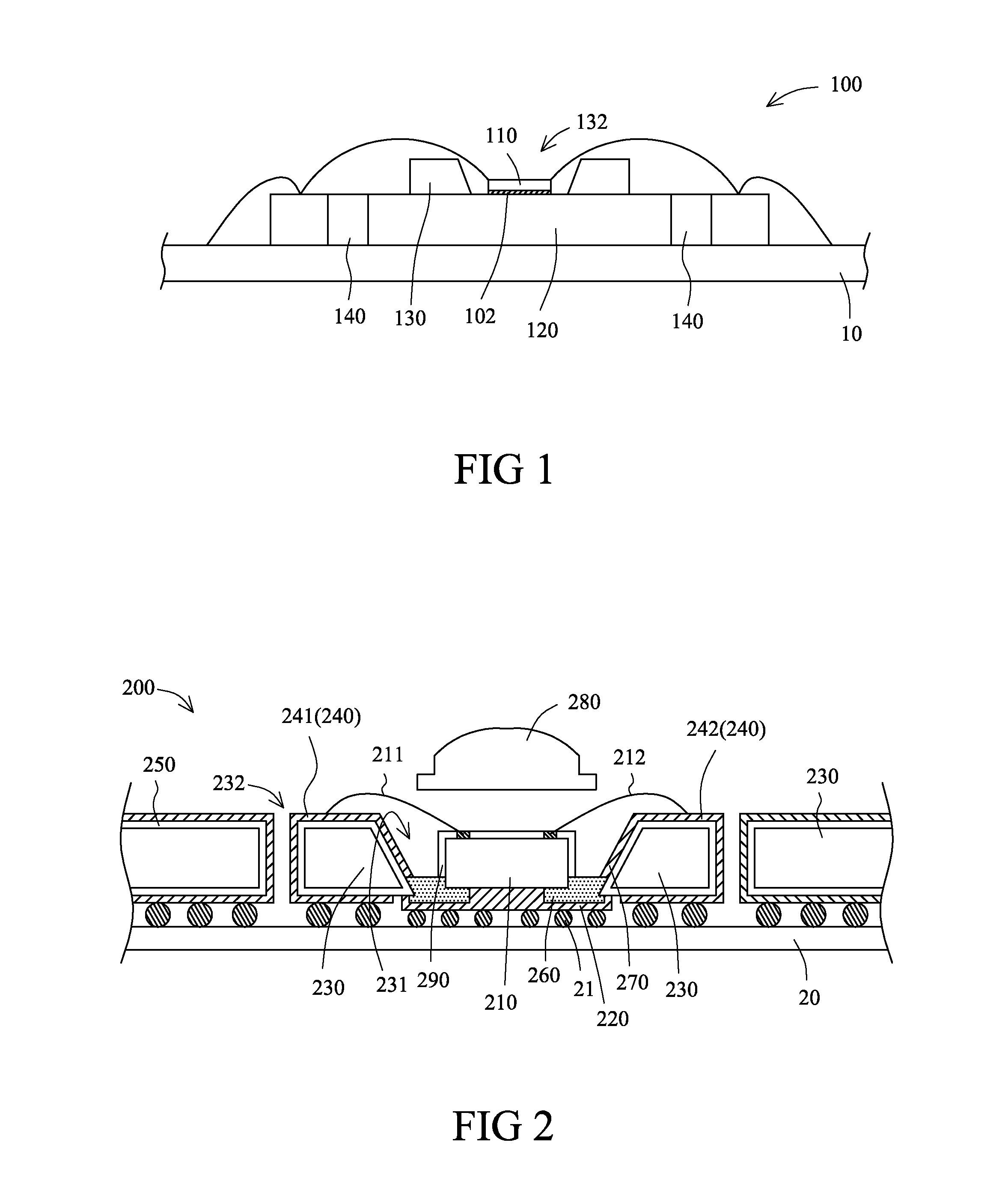
[0036]Please refer to FIG. 2 in which the LED device assembly in the present invention is shown. The LED device assembly 200 includes a light emitting diode 210, a thermally conductive film 220, a substrate 230, a plurality of conductive film patterns 240, a plurality of insulating film patterns 250, and at least one insulator 260. The thermally conductive film 220 is disposed on the bottom of the light emitting diode 210. The substrate 230 is substantially comprised of copper. A first hole 231 and a plurality of second holes 232 are disposed on the substrate 230. The first hole 231 and the second holes 232 are passed all the way through the substrate 230. The light emitting diode 210 is disposed in the first hole 231. The conductive film patterns 240 are disposed on the top surface and the bottom surface of the substrate 230, and on the side walls of the second holes 232. The thicknesses of the conductive film patterns 240 are preferably larger than 10 μm. The conductive film patte...

second embodiment

[0045]Please refer to FIG. 4 in which the LED device assembly is shown. The LED device assembly 300 includes a light emitting diode 310, a thermally conductive film 320, a substrate 330, a plurality of conductive film patterns 340, a plurality of conductive bars 350, and a plurality of insulators 360. The thermally conductive film 320 is disposed on the bottom surface of the light emitting diode 310. The substrate 330 is substantially comprised of copper. A first hole 331 and a plurality of second holes 332 are formed on the substrate. The first hole 331 and the second holes 332 are passed all the way through the substrate 330. The light emitting diode 310 is disposed in the first hole 331, and the conductive bars 350 are disposed in the second holes 332. In this embodiment, the conductive bars 350 includes a first conductive bar 351 and a second conductive bar 352. The first conductive bar 351 and the second conductive bar 352 are disposed in different second holes 332, respectivel...

third embodiment

[0053]Please refer to FIG. 6 in which the LED device assembly is shown. In this embodiment, the negative electrode of the light emitting diode 210′ is electrically connected to the first conductive film pattern 241 by wire bonding method. The positive electrode of the light emitting diode 210′ is in the bottom of the light emitting diode 210′, and contacted with the thermally conductive film 220 directly. Furthermore, the thermal conductive film 220 is not electrically connected to the first conductive film pattern 241. The thermally conductive film 220 possess the electrical conductive effect or properties, so that the second conductive film pattern is not needed to be disposed on the substrate 230, and the first hole 231 is only formed on the side of the substrate 230 on which the first conductive film pattern 241 is coated.


PUM


Abstract

A semiconductor package structure and a manufacturing method thereof are provided. The semiconductor package structure includes a semiconductor die, a thermally conductive film, a substrate, a plurality of electrically conductive film patterns, and at least one insulator. The thermally conductive film is disposed on the bottom of the semiconductor die. The substrate is substantially comprised of the electrically conductive material or semiconductor material. Furthermore, a first hole is disposed on and passed all the way through the substrate, and the semiconductor die is disposed in the first hole. The electrically conductive film patterns are disposed on the substrate, and not contacting with each other. In addition, the insulator is connected between the semiconductor die and the substrate.

Description

FIELD OF INVENTION[0001]The invention relates to a semiconductor package structure, especially relates to a semiconductor package structure having improved heat dissipation efficiency.BACKGROUND OF THE INVENTION[0002]With the rapid technological development in recent years, the luminous efficiency and the brightness of the light emitting diode is accepted by the public, so that the light emitting diode is used widely for example in backlight assembly, car lamp, and street light, etc. However, with the increasing brightness, the larger amount of heat emission from the light emitting diode has become a troublesome issue in the industry. If the heat emission cannot be removed efficiently, the brightness of the light emitting diode will be decreased and the corresponding service life will become shorter.[0003]Please refer to FIG. 1. FIG. 1 shows a front view of a traditional LED device assembly 100. The conventional LED device assembly 100 is disposed on a circuit board 10. The LED devi...

Claims


Application Information

Patent Timeline
IPC IPC(8): H01L29/41H01L21/283
CPCH01L23/3121H01L23/3677H01L2924/12041H01L2924/15311H01L2924/15153H01L23/49816H01L33/44H01L33/642H01L2224/48091H01L2933/0075H01L24/48H01L2924/01322H01L2224/73265H01L23/13H01L2224/24101H01L2224/24247H01L2924/141H01L2224/2401H01L24/24H01L24/82H01L2224/2405H01L2224/48247H01L2224/73277H01L2924/1431H01L2924/1434H01L2924/00014H01L2924/00H01L2924/15787H01L2924/12042H01L2924/12043H01L2224/45099H01L2224/45015H01L2924/207
Inventor WU, SHANG-YICHIEN, WEN-CHENGTSAI, CHIA-LUNHUANG, TIEN-HAO
Owner UNISTARS
Why Eureka
Try Eureka