Electro-optical device and electronic apparatus

a technology of optical devices and electronic devices, applied in semiconductor devices, instruments, computing, etc., can solve problems such as the fluctuation of the holding potential of the gate, and the difficulty of influencing the noise of the holding capacity, so as to prevent the deformation of the display quality

Inactive Publication Date: 2012-09-13
SEIKO EPSON CORP
View PDF9 Cites 61 Cited by
  • Summary
  • Abstract
  • Description
  • Claims
  • Application Information

AI Technical Summary

Benefits of technology

[0007]An advantage of some aspects of the invention is to prevent the display quality from

Problems solved by technology

For this reason, when there is potential fluctuation of the data line, the potential fluctuation propagates to each portion of the driving transistor, especially to the gate as a kind of noise, through parasitic capacitance, and causes the holding potential of the gate to fluctuate.
Accordingly, there was a problem in that t

Method used


Image

  • Electro-optical device and electronic apparatus
  • Electro-optical device and electronic apparatus
  • Electro-optical device and electronic apparatus

Examples


first embodiment

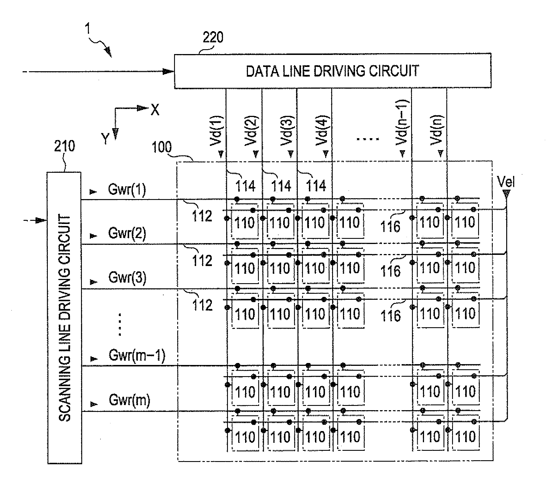
[0039]FIG. 1 is a block diagram which shows a configuration of an electro-optical device according to a first embodiment of the invention. The electro-optical device 1 is a device for displaying an image using a plurality of pixel circuits 110.

[0040]As shown in the drawing, the electro-optical device 1 includes an element unit 100, a scanning line driving circuit 210 and a data line driving circuit 220.

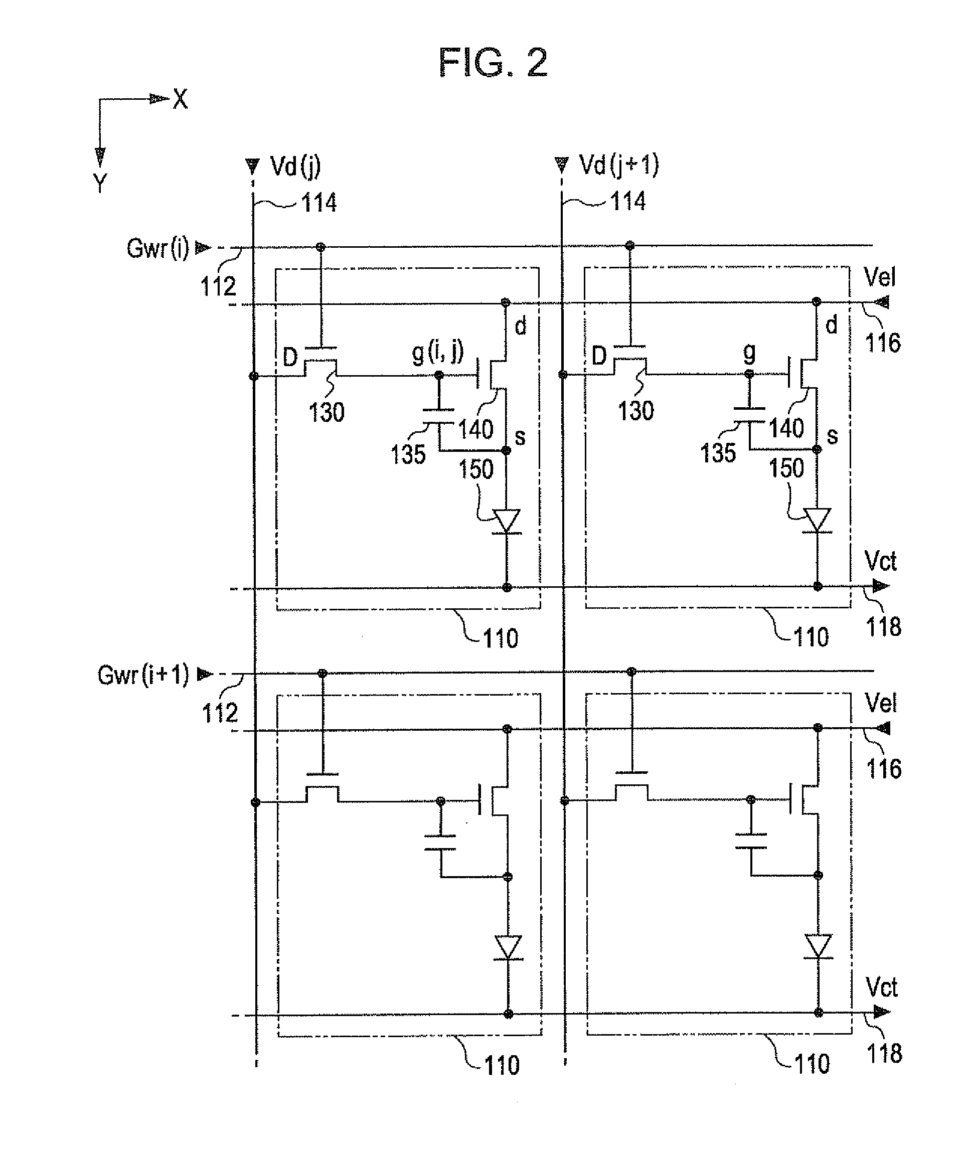
[0041]Among these, in the element unit 100, m rows of scanning lines 112 are provided in the row (X) direction, and n columns of data lines 114 are provided in the column (Y) direction in the drawing so as to maintain electrical insulation with respect to each of the scanning lines 112, each other. The pixel circuit 110 is respectively arranged corresponding to each intersection between the m rows of scantling lines 112 and the n columns of data lines 114. Accordingly, in the embodiment, the pixel circuit 110 is arranged in matrix of vertical m rows x horizontal n columns. In addition...

second embodiment

[0125]According to the first embodiment, the shield wires 81a and 81b were formed, by patterning the same wiring layer as that of the data line 114, however, the shield wires may be formed of a wiring layer different from that of the data line 114. Therefore, subsequently, as a second embodiment, an example will be described, in which the shield wires 81a and 81b are formed of the same wiring layer as that of the relay electrodes 61 and 62 which are on the lower side of the data line 114, and the power supply line 116.

[0126]FIG. 10 is a plan view which shows a configuration of a pixel circuit 110 of an electro-optical device in the second embodiment. FIG. 11 is a partial cross-sectional view of the pixel circuit shown in FIG. 10 which is cut along line XI-XI.

[0127]When forming shield wires 81a and 81b from the same wiring layer as that of relay electrodes 61 and 62, and a power supply line 116, it is necessary to avoid interference (electrical contact) from the shield wire 81a and t...

third embodiment

[0135]FIG. 12 is a plan view which shows a configuration of a pixel circuit 110 of an electro-optical device according to a third embodiment. FIG. 13 is a partial cross-sectional view of the pixel circuit in FIG. 12 which is cut along line XIII-XIII.

[0136]As shown in FIG. 12, in the third embodiment, a part of a shield wire 81a is extended toward the right side, and is formed to cover a relay electrode 43 when seen in the plan view. A holding capacity 135 is a region where the relay electrode 43 and a gate electrode layer 21 are overlapped with each other when seen in the plan view. The relay electrode 43 is the other electrode in the holding capacity 135, and also is a source node of the transistor 140. For this reason, in the third embodiment, the shielding function is further strengthened compared to the first embodiment.


PUM


Abstract

An electro-optical device includes a scanning line, a data line intersecting with each other, a pixel circuit which is provided corresponding to the intersection thereof, and a wire. The pixel circuit includes a light emitting element, one transistor which controls a current flowing to the light emitting element, and the other transistor of which conduction state is controlled according to a scanning signal which is supplied to the scanning line between a gate node of the one transistor and the data line. The wire is provided between the data line and the one transistor.

Description

[0001]This application claims priority to JP 2011-053562 filed Mar. 10, 2011, the disclosure of which is hereby incorporated by reference herein in its entirety.BACKGROUND[0002]1. Technical Field[0003]The present invention relates to an electro-optical device and an electronic apparatus.[0004]2. Related Art[0005]In recent years, various electro-optical devices in which a light emitting element such as an Organic Light Emitting Diode (hereinafter, referred to as “OLED”) is used have been proposed. In such an electro-optical device, a pixel circuit is provided corresponding to the intersection of a scanning line and a data line. In general, the pixel circuit includes the above described light emitting element, a switching transistor, and a driving transistor (refer to JP-A-2007-310311). Here, the switching transistor is turned on in a selection period of the scanning line, between the data line and a gate of the driving transistor, and in this manner, an electric potential which is su...

Claims


Application Information

Patent Timeline
IPC IPC(8): G09G5/00
CPCG09G3/3233G09G2300/0426G09G2300/043G09G2320/0209H01L27/3276H01L27/124H01L27/1255H01L27/3265H01L27/3272G09G2330/06H10K59/131H10K59/1216H10K59/126G09G3/30H10K59/1213G09G3/3266G09G3/3283G09G2300/0809
Inventor FUJITA, SHIN
Owner SEIKO EPSON CORP
Why Eureka
Try Eureka