Gate circuit

a gate circuit and gate technology, applied in the field of gate circuits, can solve the problems of surge voltage, rapid decrease of current (di/dt) in power devices, etc., and achieve the effect of slowing down the current (di/dt) and quick reducing the excessive current flowing

Active Publication Date: 2012-09-13
MITSUBISHI ELECTRIC CORP
View PDF4 Cites 21 Cited by
  • Summary
  • Abstract
  • Description
  • Claims
  • Application Information

AI Technical Summary

Benefits of technology

[0006]The present invention has been made to solve the above problems. It is, therefore, an object of the present invention to provide a gate circuit capable of quickly reducin

Problems solved by technology

This results in a rapid rate of decrease in the current (di/dt) in the p

Method used


Image

  • Gate circuit
  • Gate circuit
  • Gate circuit

Examples


first embodiment

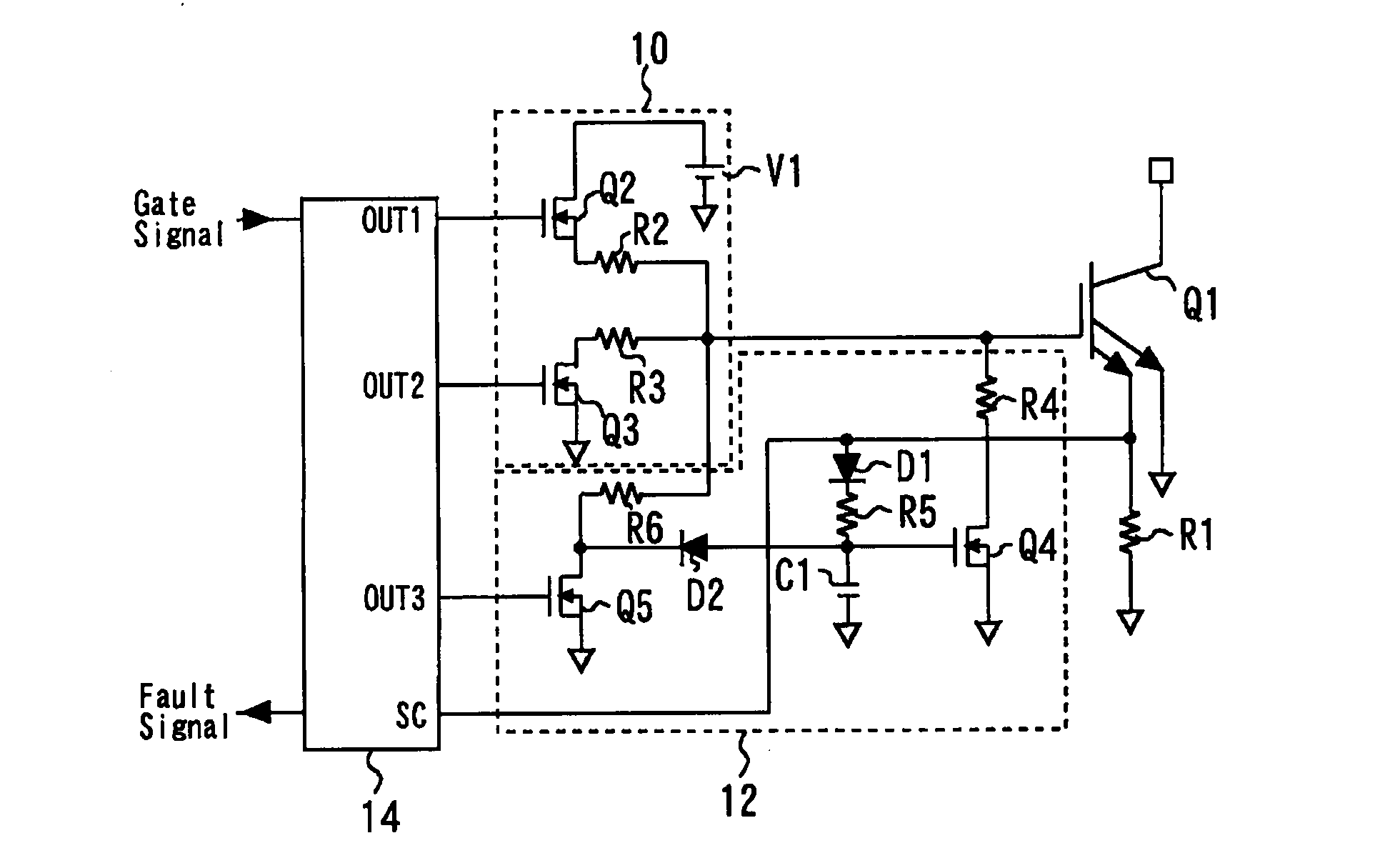
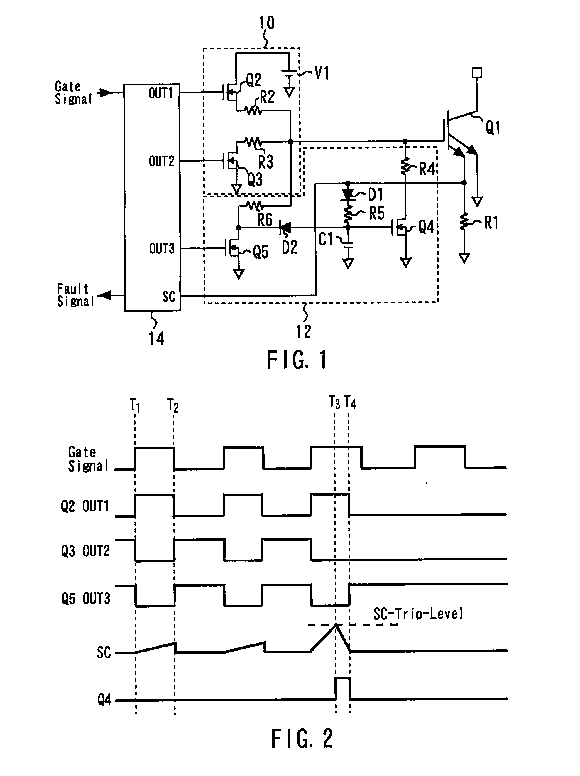
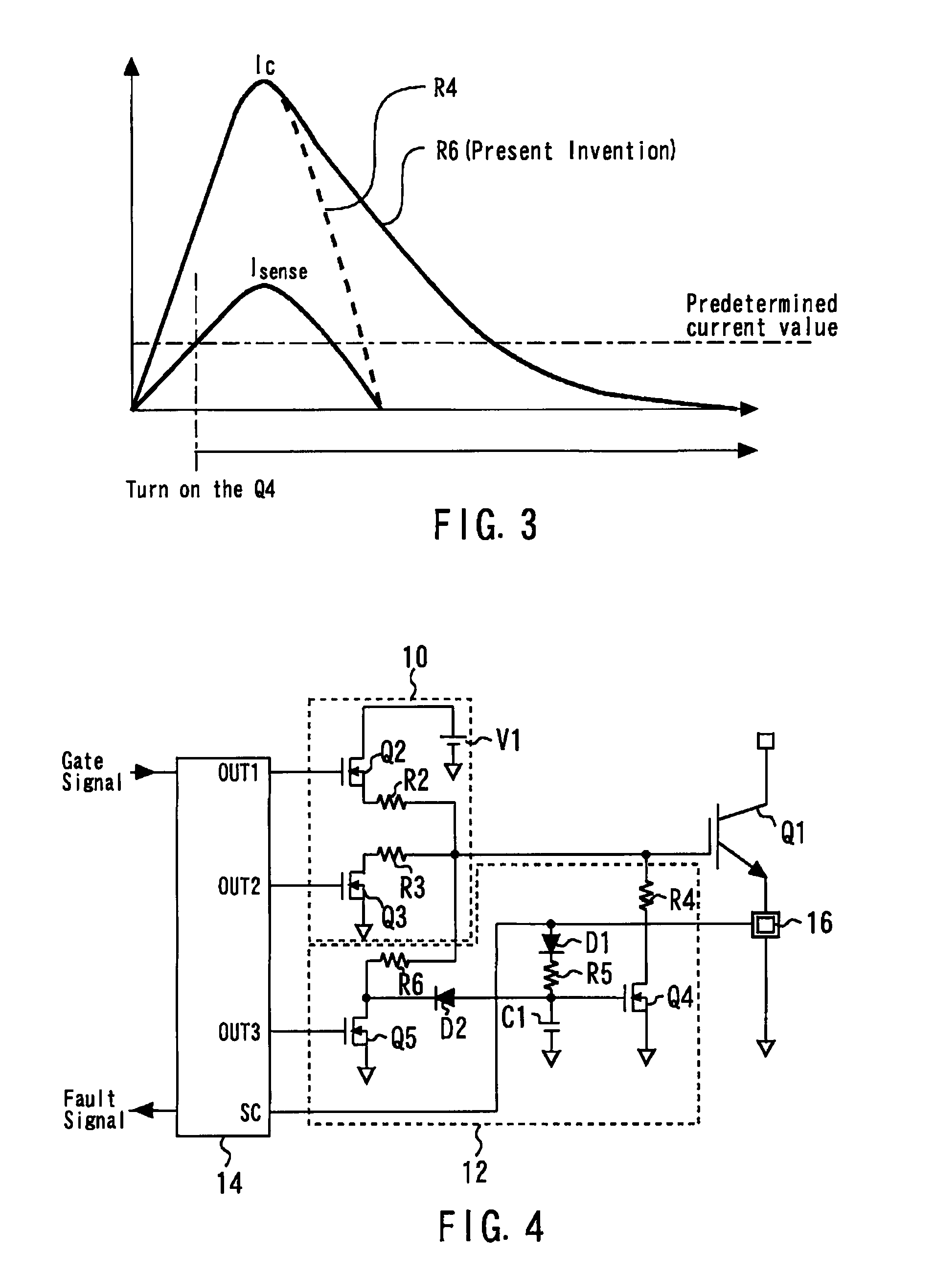
[0025]FIG. 1 is a circuit diagram of a gate circuit in accordance with a first embodiment of the present invention. The gate circuit includes a normal operation circuit 10, a protection circuit 12, and a controller integrated circuit 14. The gate circuit controls the voltage applied to the gate of a power device Q1. It should be noted that the power device Q1 is provided with an emitter sense terminal. A current detection shunt resistance R1 is connected to the emitter sense terminal. The normal operation circuit 10, the protection circuit 12, and the controller integrated circuit 14 will be described in detail.

[0026]The normal operation circuit 10 includes a gate resistive element R2 connected to the gate. An on-switching device Q2 is connected to the gate resistive element R2. The on-switching device Q2 is connected between a power supply V1 and the gate resistive element R2. That is, this on-switching device Q2 is used to permit and prevent the application of a voltage through th...

second embodiment

[0041]FIG. 6 is a circuit diagram of a gate circuit in accordance with a second embodiment of the present invention. The following description of this gate circuit will be primarily directed to the differences from the gate circuit of the first embodiment. The turn-off delay means of the gate circuit of the second embodiment is formed by discrete components. That is, this gate circuit differs from that of the first embodiment in that the controller integrated circuit is replaced by discrete components.

[0042]The gate circuit of the second embodiment includes a differential amplifier 20. The differential amplifier 20 amplifies the difference between the emitter sense voltage of the power device Q1 and the output voltage of a power supply V2. The output of the differential amplifier 20 is input to a flip-flop circuit 22. An output of the flip-flop circuit 22 is input to one input of an AND gate 24. The other input of the AND gate 24 receives the gate drive signal (Gate Signal). The out...

third embodiment

[0046]FIG. 9 is a circuit diagram of a gate circuit in accordance with a third embodiment of the present invention. In this gate circuit, two resistances are connected in parallel between the power supply V1 and the gate of the power device Q1. Specifically, these resistances are a first gate resistive element R2 and a second gate resistive element R7 having a greater resistance value than the first gate resistive element R2. A first on-switching device Q2 is connected to the first gate resistive element R2. The first on-switching device Q2 is used to permit and prevent the application of a voltage through the first gate resistive element to the gate of the power device Q1. On the other hand, a second on-switching device Q7 is connected to the second gate resistive element R7. The second on-switching device Q7 is used to permit and prevent the application of a voltage through the second gate resistive element R7 to the gate of the power device Q1.

[0047]One and of a resistive element...


PUM


Abstract

A gate circuit includes a gate resistive element connected at one end to the gate of a power device, an on-switching device connected between a power supply and the other end of the gate resistive element, a first resistive element whose connection to the gate is controlled by a first switching device, a second resistive element whose connection to the gate is controlled by a second switching device, and having a higher resistance value than the first resistive element, excessive current suppression means for turning on the first switching device just when the current in the power device reaches a predetermined value, and turn-off delay means for, after the excessive current suppression means turns on the first switching device, turning off the on-switching device and the first switching device and turning on the second switching device to turn off the power device.

Description

BACKGROUND OF THE INVENTION[0001]1. Field of the Invention[0002]The present invention relates to a gate circuit connected to the gate of a power device.[0003]2. Background Art[0004]Japanese Laid-Open Patent Publication No. 2002-353795 discloses a gate circuit connected to the gate of a power device. When an excessive current flows through the power device, this gate circuit functions so that part of the gate supply voltage appears across a resistive element. This serves to reduce the voltage actually applied to the gate of the power device, thereby reducing the excessive current in the device.[0005]In order to quickly reduce the excessive current in the power device, it is desirable to reduce the resistance value of the above resistive element. It should be noted that the power device is turned off after reducing the excessive current. In the gate circuit disclosed in the above patent publication, however, the power device is turned off by use of a resistive element of a relatively ...

Claims


Application Information

Patent Timeline
IPC IPC(8): H02H9/02
CPCH03K17/0828H03K17/18H03K17/168H03K17/163
Inventor HUSSEIN, KHALID HASSANYAMAMOTO, AKIRAWADA, FUMIO
Owner MITSUBISHI ELECTRIC CORP
Why Eureka
Try Eureka