Band gap circuit

a technology of gap circuit and output terminal, which is applied in the direction of different amplifiers, amplifiers with semiconductor devices/discharge tubes, instruments, etc., can solve the problems of poor discharging ability of resistors and diodes, difficult to remove, and reduce the stability time of voltage at the circuit output terminal. , to achieve the effect of reducing the stability time of voltage at the circuit output terminal, and reducing the cost of production

Inactive Publication Date: 2006-08-29
RENESAS ELECTRONICS CORP
View PDF16 Cites 10 Cited by
  • Summary
  • Abstract
  • Description
  • Claims
  • Application Information

AI Technical Summary

Benefits of technology

[0017]The present invention has been accomplished so as to solve such problems, and an objective thereof is to provide the band gap circuit in which the excess current can be efficiently removed that transitionally sneaks into the circuit output terminal, the PSRR is enhanced, and the stability time of the voltage at the circuit output terminal can be curtailed.
[0018]The band gap circuit relating to the present invention that is a band gap circuit for generating an output voltage to output it from a circuit output terminal, which is connected to a power supply voltage and a reference potential, comprises a differential amplifier (for example, a differential amplifier to be configured of n-channel transistors N4 and N5, and p-channel transistors P6 and P7 in embodiments of the present invention) having an inverting input terminal, a noninverting input terminal, and an output terminal; a first circuit (for example, a circuit to be configured of resistors R1 and R2, and diodes D1 and D2 in the embodiments of the present invention) for causing a potential difference to occur at said inverting input terminal and said noninverting input terminal responding to fluctuation of the voltage of said circuit output terminal; and a switching element (for example, an n-channel transistor N3 in the embodiments of the present invention) for causing the excess current of said circuit output terminal to flow in said reference potential responding to fluctuation of the potential at said output terminal of said differential amplifier, said switching element being connected to said circuit output terminal and said reference potential and being directly connected to said output terminal of said differential amplifier. Such a configuration allows the excess current, which transitionally sneaks into the circuit output terminal, to be efficiently removed.
[0019]Furthermore, the band gap circuit relating to the present invention has a first element (for example, a p-channel transistor P5 in the embodiments of the present invention) having a resistive component and a second element (for example, a resistor R2 in the embodiments of the present invention) having a capacitive component connected, wherein said first element and said second element remove power supply noise of said power supply voltage. This allows current noise of the power supply voltage to be removed, and the excess current, which transitionally sneaks into the circuit output terminal, to be removed

Problems solved by technology

As it is, discharging ability of the resistor and the diode is poor in the conventional band gap circuit, whereby the current, which flows into the output terminal VOUT at the time of introducing the power supply and of fluctuation thereof, is impossible to discharge up.
Furthermore, in the conventional band gap circuit, being accompanied by development in low power consumption, the current that flows into the output terminal VOUT at the time of introducing the power supply and of fluctuation thereof is impossible to discharge up, whereby the problem exists that a stability time of the voltage at the output terminal VOUT at the

Method used


Image

  • Band gap circuit
  • Band gap circuit
  • Band gap circuit

Examples


embodiment 1

OF THE INVENTION

[0037]In the embodiment 1 of the present invention (hereinafter, called the embodiment 1 for short), the band gap circuit having no low-pass filter will be explained.

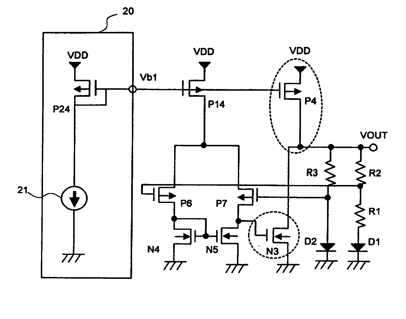
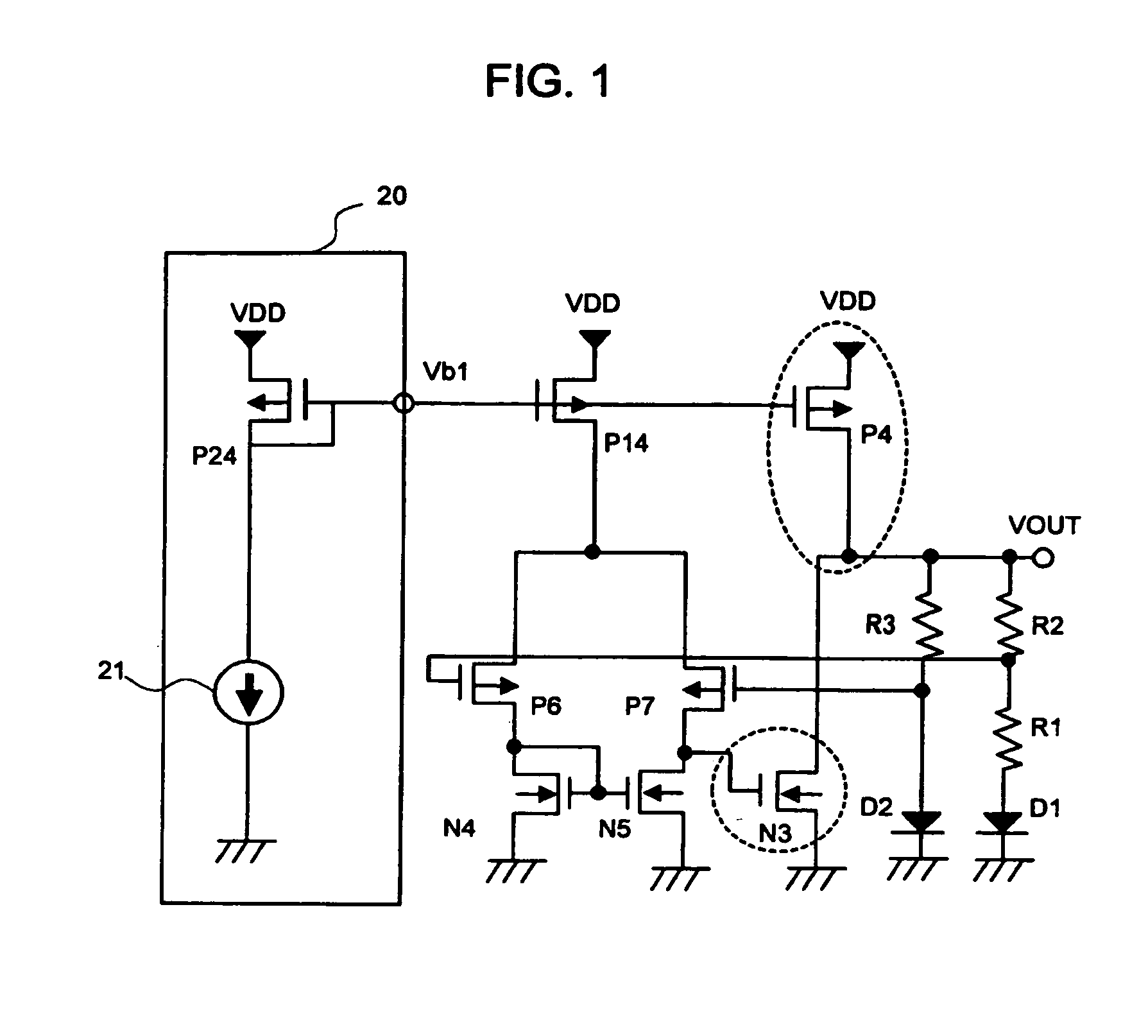
[0038]At first, a configuration of the band gap circuit in the embodiment 1 will be explained by employing FIG. 1. FIG. 1 is a schematic circuit diagram illustrating one configuration example of the band gap circuit in the embodiment 1. As shown in FIG. 1, the band gap circuit in the embodiment 1 has the differential amplifier, and the n-channel transistor N3 connected to this differential amplifier. Additionally, hereinafter, the n-channel transistor is called an n-type transistor for short, and the p-channel transistor called a p-type transistor.

[0039]The differential amplifier is configured of a general op-amp. As shown in FIG. 1, the differential amplifier of the band gap circuit is configured of one pair of p-type transistors P6 and P7, and one pair of n-type transistors N4 and N5.

[0040]A source of ...

embodiment 2

THE INVENTION

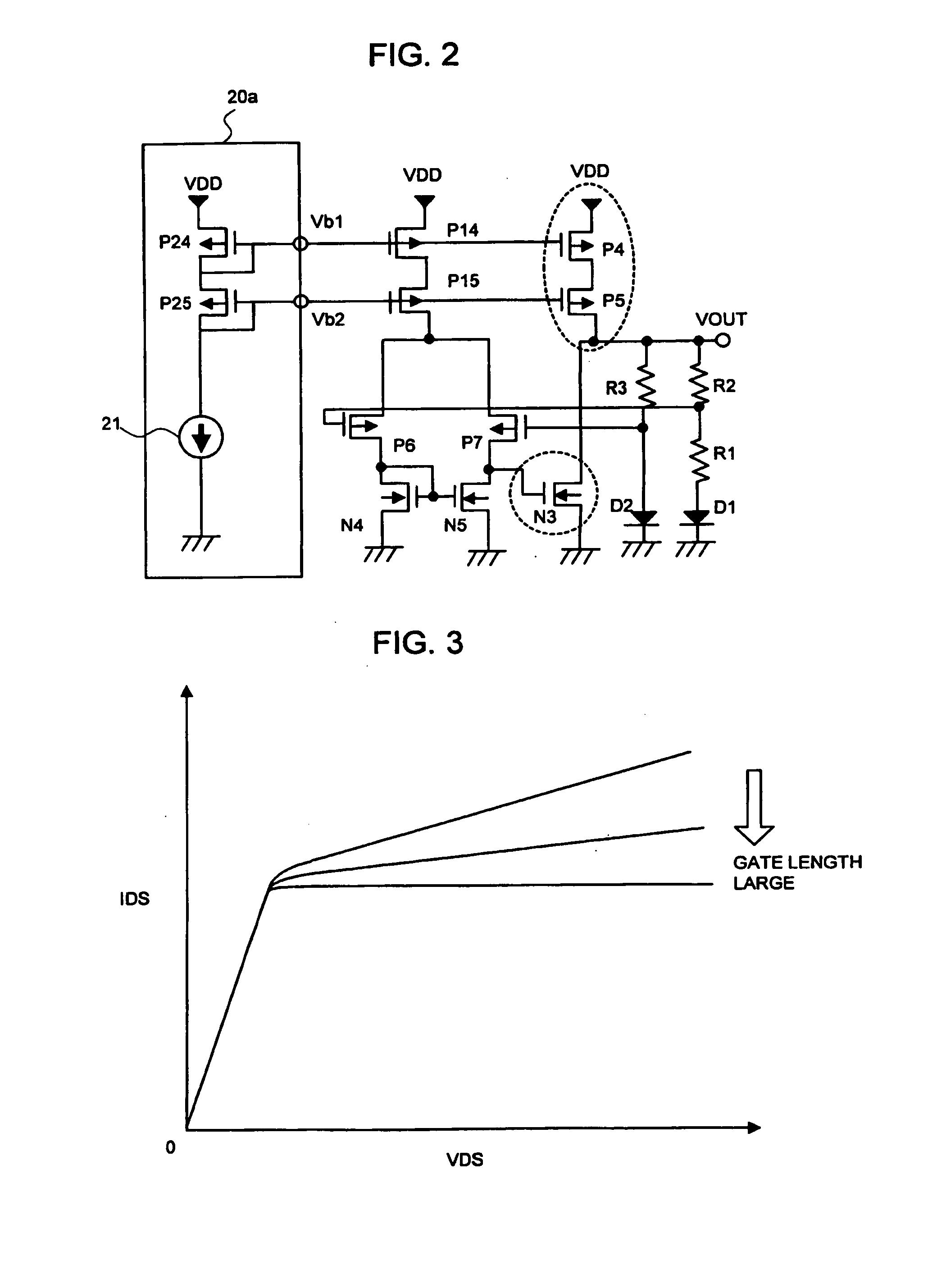
[0081]In the embodiment 2 of the invention (hereinafter, called the embodiment 2 for short), the band gap circuit having a low-pass filter provided will be explained.

[0082]At first, a configuration of the band gap circuit in the embodiment 2 will be explained by employing FIG. 2. FIG. 2 is a schematic circuit diagram illustrating one configuration example of the band gap circuit in the embodiment 2. As shown in FIG. 2, the band gap circuit in the embodiment 2 is configured similarly to the band gap circuit in the embodiment 1. And, the band gap circuit in the embodiment 2 has the p-type transistor P5 further connected between the output terminal VOUT of the band gap circuit and the p-type transistor P4. Additionally, herein, is omitted the explanation on the differential amplifier, the n-type transistor N3, the p-type transistor P4, etc. that are similar to that of the embodiment 1.

[0083]The p-type transistor P5 has the drain thereof connected to the output terminal VOU...


PUM


Abstract

A band gap circuit, including a differential amplifier. In response to fluctuation of the voltage on the band gap circuit output terminal VOUT, a potential difference occurs at an inverting input terminal and a noninverting input terminal of the differential amplifier. A transistor, connected to the output terminal VOUT, ground, an output terminal of the differential amplifier, causes excess current from the output terminal VOUT to flow to ground in response to fluctuation of the potential at the output terminal of the differential amplifier. A transistor that has a resistive component and a resistor that has a capacitive component are connected between a power supply voltage VDD and the output terminal VOUT.

Description

BACKGROUND OF THE INVENTION[0001]The present invention relates to a band gap circuit in which an operation is performed in a high-frequency region by employing a low-voltage power supply.[0002]Conventionally, a semiconductor integrated circuit is provided with a reference voltage generation circuit for stably generating a reference voltage for use in a D / A converter etc. As to the reference voltage generation circuit, there is a band gap circuit in which a difference of a threshold voltage of a transistor is utilized. The band gap circuit prevents the semiconductor integrated circuit from malfunctioning due to the rising of the voltage that occurs at the time of introducing the power supply of the semiconductor integrated circuit, and fluctuation etc. of a power supply voltage that occurs during the operation, and reduces power supply voltage dependency of the semiconductor integrated circuit. Also, this band gap circuit also generates the reference voltage stabilized against temper...

Claims


Application Information

Patent Timeline
IPC IPC(8): G05F1/575G05F1/46G05F3/24G05F3/26G05F3/30H03F3/347H03F3/45
CPCG05F3/30G05F3/26
Inventor ABE, OSAMU
Owner RENESAS ELECTRONICS CORP
Why Eureka
Try Eureka