
Display substrate, display apparatus having the same and method of manufacturing the same

a technology of display apparatus and substrate, which is applied in the field of display apparatus having the display substrate, can solve the problems of reducing reflectance, limiting the use of chrome (cr), and polluting the etching chamber, so as to achieve uniformity, reduce the effect of light utilization efficiency and a display quality

Active Publication Date: 2012-09-20
TCL CHINA STAR OPTOELECTRONICS TECH CO LTD
View PDF5 Cites 16 Cited by
  • Summary
  • Abstract
  • Description
  • Claims
  • Application Information

AI Technical Summary

Benefits of technology

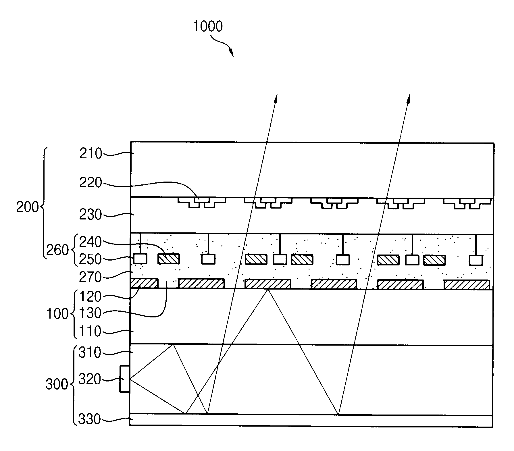
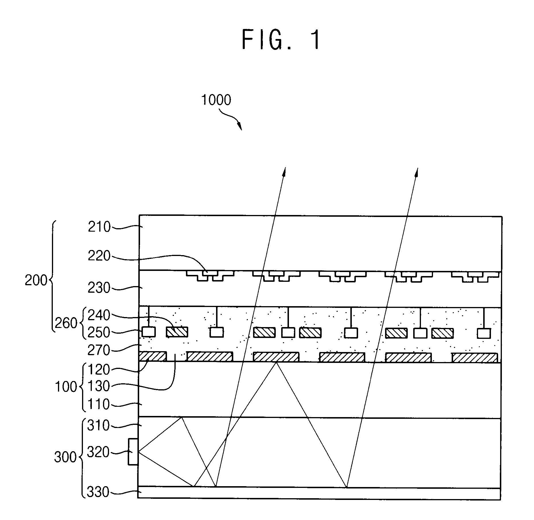
[0010]Example embodiments of the invention provide a display substrate capable of enhancing a light utilizing efficiency and a display quality.
[0036]According to example embodiments, a light utilizing efficiency and a display quality may be increased.
[0037]For the high reflective layer, double layers of silicon nitride (SiNx) and silicon oxide (SiOx) are deposited at three times to increase a reflectance, and a thickness of a first silicon nitride (SiNx) layer is deposited larger than a thickness of each of the other silicon nitride (SiNx) layers, so that an area in which the reflectance is uniform may be increased in a visible-ray region. Accordingly, even if a thickness error occurs during a manufacturing process, the reflectance may be less changed.
[0038]In addition, heavy metals such as chrome (Cr) are replaced with a multi-layered film formed using silicon nitride (SiNx) and titanium (Ti), so that a low reflectance is more uniformized and pollution due to harmful heavy metals may be decreased.
[0039]In addition, etching a thick stacked reflective layer to form an opening slot is divided into two processes or steps, and the contact hole is patterned at the same time of forming the opening slot in a second etching, so that a processing error may be decreased.

Problems solved by technology

The high reflective layer may have a stacked structure to embody a high reflectance, but the reflectance may be decreased according to an emitting wavelength band, due to an error of a stacked thickness occurring in depositing a stacked layer.
In this case, an etching chamber may be polluted due to particles generated during an etching process.
Furthermore, using a heavy metal such as chrome (Cr) may be restricted according to increasing demands for an environment-friendly product in the industrial field.
When the reflective layer is relatively thick due to the stacked structure, an error may be increased during a process of forming the opening slots.

Method used


Image

  • Display substrate, display apparatus having the same and method of manufacturing the same
  • Display substrate, display apparatus having the same and method of manufacturing the same
  • Display substrate, display apparatus having the same and method of manufacturing the same

Examples


Embodiment Construction

[0048]The invention is described more fully hereinafter with reference to the accompanying drawings, in which example embodiments of the invention are shown. This invention may, however, be embodied in many different forms and should not be construed as limited to the example embodiments set forth herein. Rather, these embodiments are provided so that this disclosure will be thorough and complete, and will fully convey the scope of the invention to those skilled in the art. In the drawings, the size and relative sizes of layers and regions may be exaggerated for clarity.

[0049]It will be understood that when an element or layer is referred to as being “on” and “connected to” another element or layer, the element or layer can be directly on or connected to another element or layer or intervening elements or layers. In contrast, when an element is referred to as being “directly on” or “directly connected to” another element or layer, there are no intervening elements or layers present....


PUM

PropertyMeasurementUnit
refractive indexaaaaaaaaaa
thicknessaaaaaaaaaa

Abstract

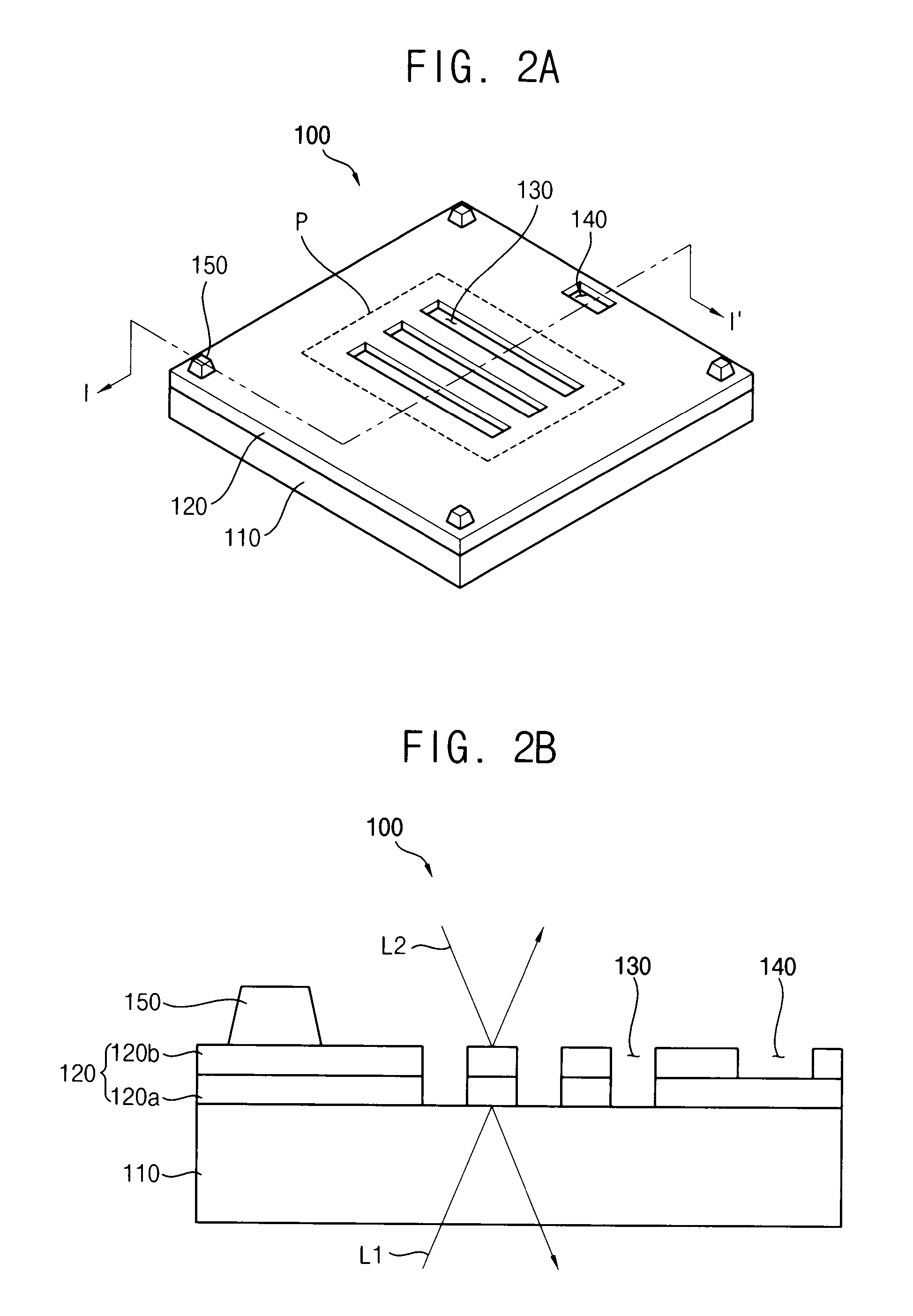
A display substrate includes a base substrate, a high reflective layer, a metal light reflective layer and a low reflective layer. The high reflective layer is on the base substrate, and includes a high refractive layer and a low refractive layer which alternate with each other. The high refractive layer has a first refractive index, and the low refractive layer has a second refractive index smaller than the first refractive index. The metal light reflective layer is between the high reflective layer and the low reflective layer, and reflects a light. The low reflective layer comprises a light absorbing layer which absorbs a light, and at least one insulating layer. Accordingly, a light utilizing efficiency and a display quality may be increased.

Description

CROSS REFERENCE TO RELATED APPLICATION[0001]This application claims priority under 35 U.S.C. §119 to Korean Patent Application No. 2011-0024267, filed on Mar. 18, 2011 in the Korean Intellectual Property Office (KIPO), the contents of which are herein incorporated by reference in their entireties.BACKGROUND OF THE INVENTION[0002]1. Field of the Invention[0003]Example embodiments of the invention relate to a display substrate, a display apparatus having the display substrate and a method of manufacturing the display substrate. More particularly, example embodiments of the invention relate to a display substrate based on a micro electro-mechanical system (“MEMS”), a display apparatus having the display substrate and a method of manufacturing the display substrate.[0004]2. Description of the Related Art[0005]Conventionally, display apparatuses such as a liquid crystal display (“LCD”), a plasma display panel (“PDP”), and a field emission display (“FED”) have been used, and a research on...

Claims


Application Information

Patent Timeline
Patent Type & Authority Applications(United States)
IPC IPC(8): G02B26/02G02B5/22C23C16/40C23C16/34B05D3/10G02B1/10B05D5/06
CPCG02B26/02G02B5/085G02B5/003
Inventor YUN, SUNG-SIKPARK, JAE-BYUNGBYUN, JIN-SEOBCHO, HYUN-MINKIM, YU-KWAN
Owner TCL CHINA STAR OPTOELECTRONICS TECH CO LTD
Learn More