Ultra-High Voltage N-Type-Metal-Oxide-Semiconductor (UHV NMOS) Device and Methods of Manufacturing the same
a technology of metal-oxide-semiconductor and ultra-high voltage, which is applied in the direction of semiconductor devices, electrical equipment, transistors, etc., can solve the problems that the use of low-voltage complementary metal-oxide-semiconductor (cmos) technologies for these dual functions may not be practical, and achieves the effect of improving performance and being easy to carry ou
- Summary
- Abstract
- Description
- Claims
- Application Information
AI Technical Summary
Benefits of technology
Problems solved by technology
Method used
Image

Examples
first embodiment
UHV NMOS Device of First Embodiment
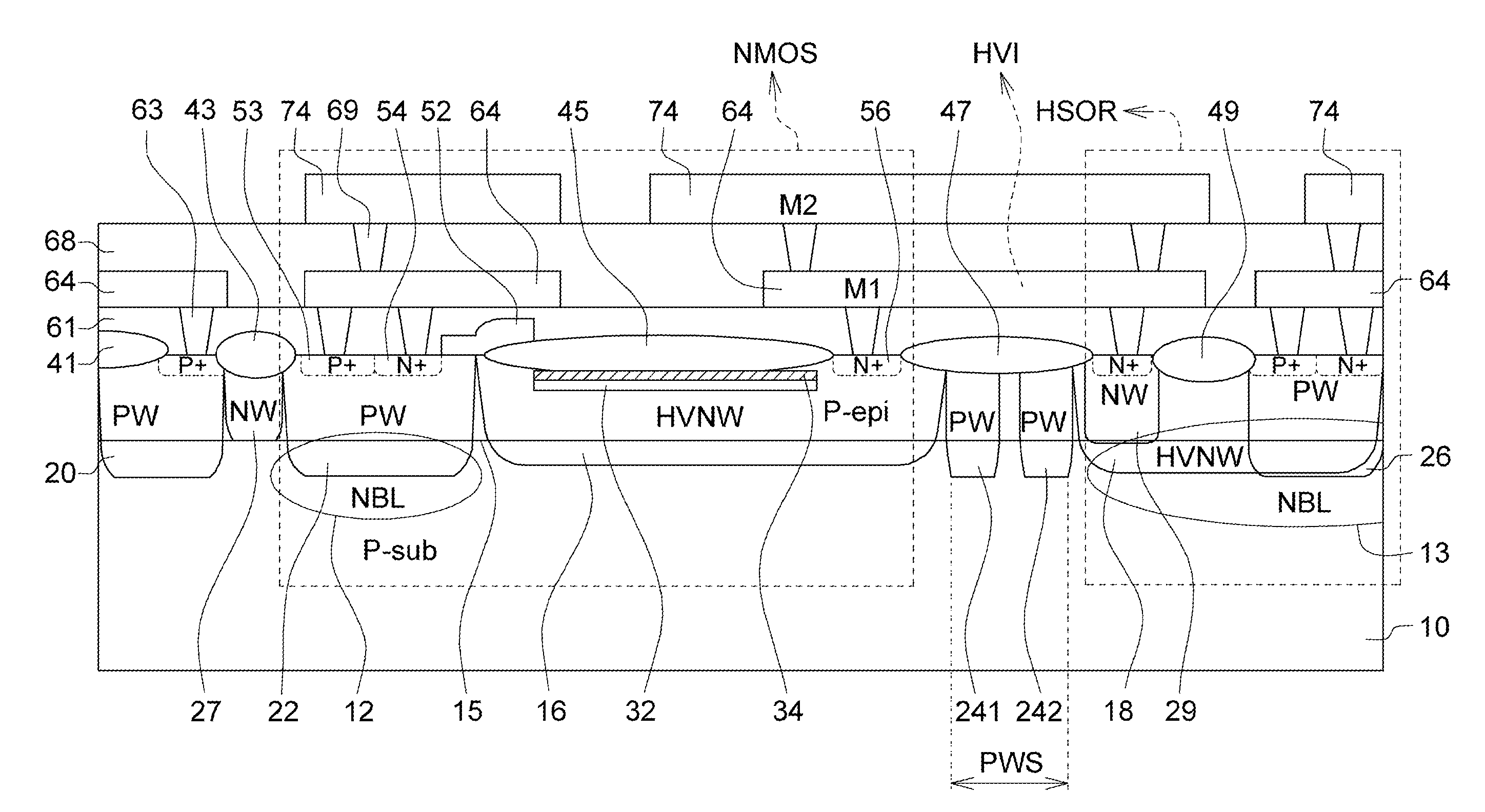
[0033]FIG. 1 shows an ultra-high voltage n-type-metal-oxide-semiconductor (UHV NMOS) device according to the first embodiment of the present disclosure. In the first embodiment, an UHV NMOS device includes a substrate 10, such as a P-substrate. As shown in FIG. 1, the substrate 10 includes a NMOS region and a high-side operation region (HSOR). The UHV NMOS device further includes a first N-doped buried layer (NBL) 12 disposed at the NMOS region and a second NBL 13 disposed at the high-side operation region for providing isolation functionality. In the embodiment, a P-epi layer 15 could be optionally deposited over the substrate 10. The UHV NMOS device further includes a first high-voltage N-well (HVNW) region 16 disposed in a portion of the substrate 10 and a second HVNW region 18 disposed in a high-side operation region (HSOR) of the substrate 10. The first and second HVNW regions 16 and 18 may provide an increased critical electrical field for pr...
second embodiment
UHV NMOS Device of Second Embodiment
[0048]FIG. 5 shows an ultra-high voltage n-type-metal-oxide-semiconductor (UHV NMOS) device according to the second embodiment of the present disclosure. In the second embodiment, the device may include one metallic layer instead of two. Please refer to FIG. 1 and FIG. 5 together. The devices of FIG. 5 and FIG. 1 are identical, except two metallic layers of FIG. 1 is reduced to one metallic layer (i.e. the first patterned metal layers 64) of FIG. 5.
third embodiment
UHV NMOS Device of Third Embodiment
[0049]FIG. 6 shows an ultra-high voltage n-type-metal-oxide-semiconductor (UHV NMOS) device according to the third embodiment of the present disclosure. In the third embodiment, the N-doped buried layer (NBL) of the device could be optionally removed in order to provide different applications. Please refer to FIG. 1 and FIG. 6 together. The devices of FIG. 6 and FIG. 1 are identical, except the first NBL 12 at the source side of FIG. 1 is removed, and not shown in the device of FIG. 6.
PUM
 Abstract
Description
Claims
Application Information
 - Generate Ideas
- Intellectual Property
- Life Sciences
- Materials
- Tech Scout
- Unparalleled Data Quality
- Higher Quality Content
- 60% Fewer Hallucinations
Browse by: Latest US Patents, China's latest patents, Technical Efficacy Thesaurus, Application Domain, Technology Topic, Popular Technical Reports.
© 2025 PatSnap. All rights reserved.Legal|Privacy policy|Modern Slavery Act Transparency Statement|Sitemap|About US| Contact US: help@patsnap.com