Electro-optic device and method for manufacturing same

a technology of electro-optic devices and manufacturing methods, applied in thermoelectric devices, organic semiconductor devices, instruments, etc., to achieve the effects of reducing the size and thickness of conductive wiring boards, reducing takt time and fabrication costs, and reducing the size and thickness of electro-optic devices

Inactive Publication Date: 2012-09-27
SHARP KK
View PDF0 Cites 3 Cited by
  • Summary
  • Abstract
  • Description
  • Claims
  • Application Information

AI Technical Summary

Benefits of technology

[0039]According to the present invention, the plurality of conductive wires are arranged on one surface so as not to intersect with each other. Therefore, it is possible to reduce the size and the thickness of the conductive wiring board, compared to the case where the conductive wires are layered in a multilayer structure. If the conductive wires are layered in a multilayer structure, it is necessary to provide an insulating layer for separating the layered conductive wires from one another. However, since the plurality of conductive wires do not intersect with each other, and are provided in a single layer, a step of forming the insulating layer can be omitted, and moreover, the conductive wires can be obtained by performing a step, e.g., photolithography, only once. Accordingly, it is possible to reduce the takt time and fabrication costs. Further; insulating base members are provided on the surfaces of the plurality of optical elements which face the conductive wiring board. Therefore, even in the case where the plurality of conductive wires are arranged so as not to intersect with each other, and are provided in a single layer, it is possible to obtain a conductive wiring board with a complex conductive pattern by connecting the lower electrode with one of the plurality of conductive wires, and connecting the upper electrode with a conductive wire different from the one connected to the lower electrode. Thus, it is possible to reduce the size and the thickness of the electro-optic device as a whole, which is fabricated using the conductive wiring board provided with a plurality of conductive wires arranged so as not to intersect with each other.

Problems solved by technology

With higher complexity and higher definition of the electro-optic devices, more wires need to be provided on a mounting board.

Method used


Image

  • Electro-optic device and method for manufacturing same
  • Electro-optic device and method for manufacturing same
  • Electro-optic device and method for manufacturing same

Examples


first embodiment

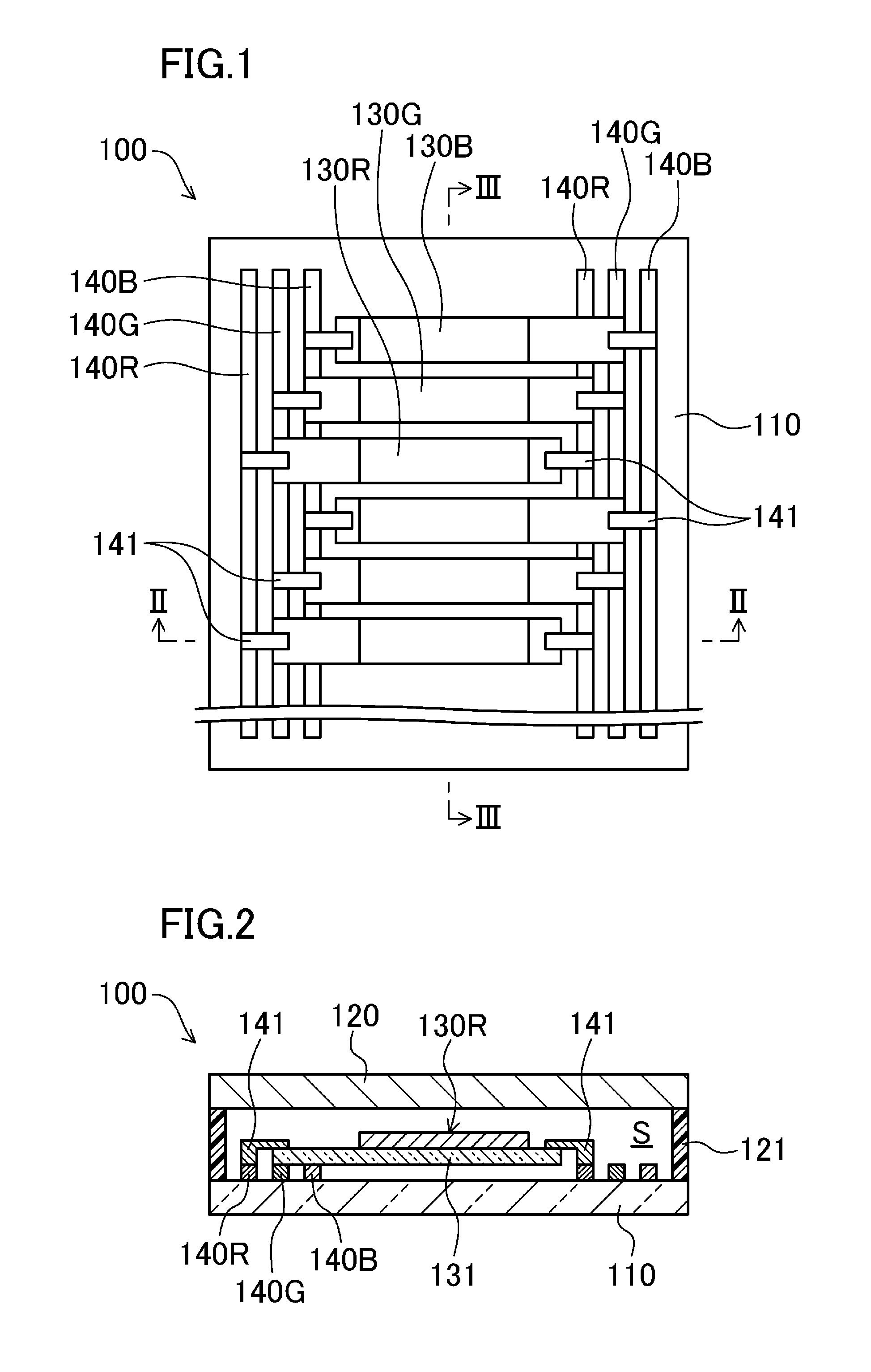
[0052]An organic EL illuminating device as an embodiment of an electro-optic device will be described in detail below, based on the drawings. FIGS. 1-3 show an organic EL illuminating device 100 according to the first embodiment. The organic EL illuminating device 100 is used, for example, as office lighting, store lighting, facility lighting, stage lighting and set lighting, exterior lighting, residential lighting, display lighting (used, for example, for a pachinko machine, a vending machine, and a freezer / refrigerator showcase), lighting such as built-in lighting in equipment / furniture, a liquid crystal panel backlight, illuminations, neon, a luminous source for signs.

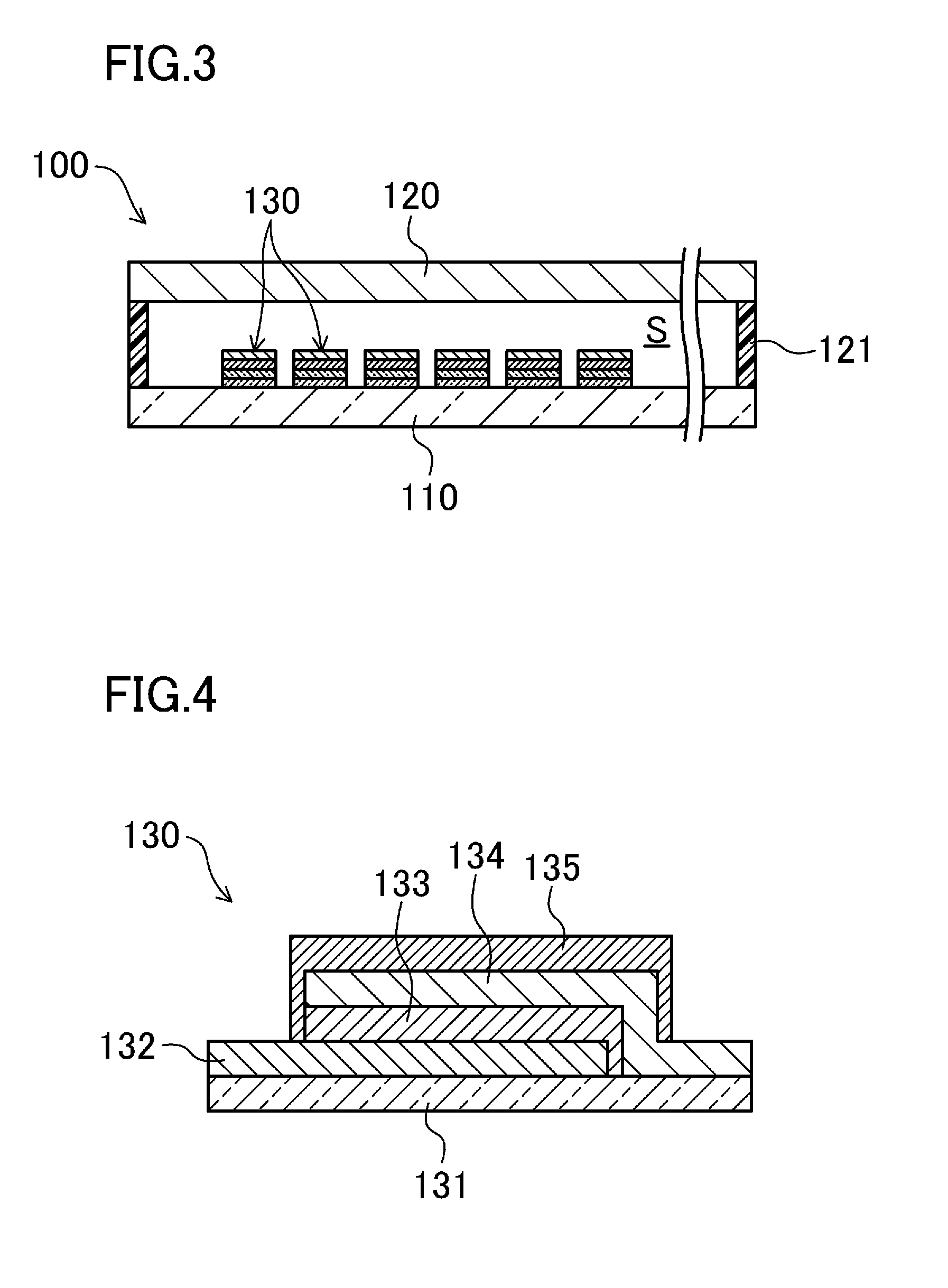
[0053]The organic EL illuminating device 100 has a structure in which a first substrate 110 and a second substrate 120 are provided to face each other, and a plurality of organic EL illuminators 130 are provided on a surface of the first substrate 110 in the enclosed space S formed between the substrates.

[0054]Here,...

second embodiment

[0124]FIG. 11 shows a liquid crystal display device 200 according to the second embodiment. The liquid crystal display device 200 is used, for example, as a large display for a television, a small display for a portable device, etc.

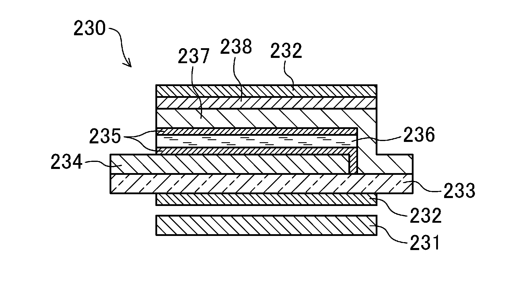
[0125]The liquid crystal display device 200 has a structure in which a plurality of liquid crystal display elements 230 are located in an enclosed space S formed between a first substrate 210 and a second substrate 220.

[0126]In the liquid crystal display device 200, the liquid crystal display element 230 serves as one pixel. The display device may be capable of higher-definition display by providing a TFT on an illuminator and providing a plurality of pixels capable of being driven independently from one another in one liquid crystal display element 230.

[0127]The first substrate 210 and the second substrate 220 are made of materials similar to the materials of the first and second substrates of the organic EL illuminating device 100 according to the first...

example 1

[0133]An organic EL illuminating device having a structure described in the first embodiment was fabricated. Here, each of the organic EL illuminators has a strip shape whose length is 160 mm and a width is 30 mm. Three types of illuminators, i.e., a red color illuminator, a green color illuminator, and a blue color illuminator, were prepared.

[0134]Glass substrates each having a length of 200 mm, a width of 200 mm, and a thickness of 0.7 mm were used as the first substrate and the second substrate. Conductive wires were formed on a surface of the first substrate in an atmosphere in which a degree of vacuum is 6×10⁻⁴ Pa. The thickness of each of the wires was 100 nm.

[0135]Voltages were applied to the respective conductive wires such that the illumination percentages of the red color illuminator, the green color illuminator, and the blue color illuminator would be 30%, 22%, and 48%, respectively. Here, the term “illumination percentage” refers to a percentage to a maximum current flow...


PUM

PropertyMeasurementUnit
thicknessaaaaaaaaaa
lengthaaaaaaaaaa
lengthaaaaaaaaaa

Abstract

An electro-optic device (100) includes a conductive wiring board (110) on one surface of which a plurality of conductive wires (140) are arranged so as not to intersect with each other, and a plurality of optical elements (130) each of which is provided on the board (110), and in which an insulating base member (131), a lower electrode (132), a function layer (133), and an upper electrode (134) are sequentially formed on the board (110). In this device (100), the lower electrode (132) is electrically connected to one of the conductive wires (140); the upper electrode (134) is electrically connected to one of the conductive wires (140) which is not connected to the lower electrode (132); and each of the optical elements (130) is provided such that part of the optical element (130) overlaps with part of one or more of the conductive wires (140) in plan view.

Description

TECHNICAL FIELD[0001]The present invention relates to electro-optic devices, such as organic EL devices and liquid crystal display devices which have a conductive wiring board, and methods for manufacturing the electro-optic devices.BACKGROUND ART[0002]Examples of the electro-optic devices which can be used as a flat-type light source include, for example, illuminating devices such as an organic EL illuminating device, an inorganic EL illuminating device, a plasma illuminating device, and a field emission lamp (FEL), and display devices such as a liquid crystal display device, an organic EL display device, an inorganic EL display device, a plasma display device, an electrophoretic display (EPD) device, and a field emission display (FED) device.[0003]With higher complexity and higher definition of the electro-optic devices, more wires need to be provided on a mounting board. Thus, conductive wires are formed in a multilayer structure by alternately layering a conductive wire and an i...

Claims


Application Information

Patent Timeline
Patent Type & Authority Applications(United States)
IPC IPC(8): H01L51/52G02F1/1337H01L51/56
CPCH01L51/0085H01L51/5203H05B33/10H05B33/06H01L2251/5361H10K85/342H10K50/805
Inventor YAMADA, MAKOTOFUJITA, YOSHIMASA
Owner SHARP KK
Why Eureka
Try Eureka