Low power compact optical switch

a compact, optical switch technology, applied in the field of optical waveguide switches, can solve the problems of reducing the refractive index of the waveguide, the relative complexity of the semiconductor device, and the limit of the switching angle, and achieve the effect of reducing the change in the waveguide refractive index

Inactive Publication Date: 2012-09-27
HER MAJESTY THE QUEEN & RIGHT OF CANADA REPRESENTED BY THE MIN OF IND THROUGH THE COMM RES CENT
View PDF10 Cites 10 Cited by
  • Summary
  • Abstract
  • Description
  • Claims
  • Application Information

AI Technical Summary

Benefits of technology

[0010]The present invention relates to optical waveguide switches having a multi-reflection switching electrode for reducing the change in the waveguide refractive index that is required for switching the direction of propagation of input light by a given angle.

Problems solved by technology

Typically, achieving such carrier confinement involves using relatively complex semiconductor device technologies, such as ion implantation, electron-beam lithography, Zn diffusion, and epitaxial regrowth.
One drawback of the design of FIG. 1 is that, for optimal performance, the electrode 30 should be positioned with its ‘receiving’ edge 31 centered in the common waveguide region 15.
One disadvantage of the prior art semiconductor switches is that they are limited to small switching angles, or equivalently a small waveguide crossing angle, typically about 2° or less for a 2×2 switch, and 4° or less for a 1×2 switch.
The small switching angle increases the size of the device and limits the integration density.
Another disadvantage of the prior art TIR semiconductor switches is their relatively large power consumption, especially for devices with the switching angle at the higher end of the range, as such devices require larger electrical currents.

Method used


Image

  • Low power compact optical switch
  • Low power compact optical switch
  • Low power compact optical switch

Examples


Embodiment Construction

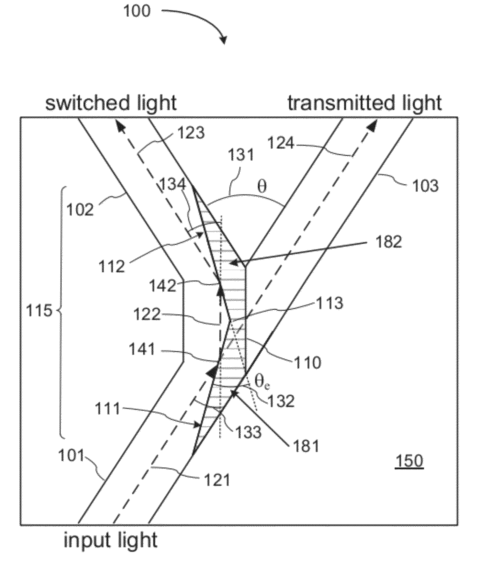
[0028]With reference to FIG. 3, there is illustrated, in a plane view, an optical switching structure (OSS) 100 employing a double-reflection electrode geometry according to an embodiment of the present invention. In the shown embodiment the OSS 100 utilizes a ‘Y’-shaped waveguide structure that is well known in the art. It has an input waveguide 101, hereinafter also referred to as the first input waveguide, a first output waveguide 103, and a second output waveguide 102. A waveguide branching region 115 optically couples the first input waveguide 101 to one of the output waveguides 102 and 103. At the waveguide branching region 115, the second output waveguide 102 is oriented at angle θ131 with respect to the first output waveguide 103 and the first input waveguide 101. The angle 131θ is referred to herein as the branching angle, crossing angle or light switching angle. The waveguide branching region 115 may be viewed as, or includes, a common, or shared, portion of the input and ...


PUM


Abstract

The invention relates to optical waveguide switches wherein input light propagating in an input waveguide may be switched between two output waveguides by means of a carrier-induced total internal reflection. The switches utilizes a double-reflection, or, generally, a multiple-reflection electrode to reduce the light deflection angle at each reflection interface, thereby enabling to increase the light switching angle and / or decrease the power consumption of the switch.

Description

TECHNICAL FIELD[0001]The present invention relates to optical switches, and in particular to optical waveguide switches having an electrode at a waveguide branching point for switching the direction of light propagation by applying an electrical signal to the electrode.BACKGROUND OF THE INVENTION[0002]Fast optical switching is an important enabler of advanced optical networks, in particular such functions as routing burst and packet optical signals, optical path provisioning and fault restoration. Semiconductor digital optical switches (DOSs) can fulfill such high speed applications due to their nanosecond switching times, step-like switching responses, and robustness to variations in temperature, wavelength, polarization, refractive index and device fabrication tolerances. Moreover, semiconductor optical switches offer potential for integration with other semiconductor components, both optical and electronic, and thus promise considerable savings in the size, complexity and cost of...

Claims


Application Information

Patent Timeline
Patent Type & Authority Applications(United States)
IPC IPC(8): G02B6/35
CPCG02B6/3536G02F2201/122G02F1/3138
Inventor SUN, LIPINGCAO, SHAOCHUNSAVOIE, MICHEL
Owner HER MAJESTY THE QUEEN & RIGHT OF CANADA REPRESENTED BY THE MIN OF IND THROUGH THE COMM RES CENT
Why Eureka
Try Eureka