High performance surface mount electrical interconnect with external biased normal force loading

a surface mount and normal force technology, applied in the direction of resistive material coating, fixed capacitor details, coupling device connections, etc., to achieve the effect of reliable connection, low force, and stable contact resistan

Active Publication Date: 2012-09-27
HSIO TECH
View PDF13 Cites 73 Cited by
  • Summary
  • Abstract
  • Description
  • Claims
  • Application Information

AI Technical Summary

Benefits of technology

[0015]The challenge with this type of product is to create an interface between the solder ball on the device and the contact tips such that the device can be inserted with low enough force to enable insertion by hand, while still providing stable contact resistance and reliable connection. Related to this challenge is the extraction force relative to insertion force such that the device can be easily removed by hand or with the aid of a tool without breaking solder joints between the contact and the PCB as well as the joint from the device to the solder ball on the package.
[0022]The use of additive printing processes permits the material set in a given layer to vary. Traditional PCB and flex circuit fabrication methods take sheets of material and stack them up, laminate, and / or drill. The materials in each layer are limited to the materials in a particular sheet. Additive printing technologies permit a wide variety of materials to be applied on a layer with a registration relative to the features of the previous layer. Selective addition of conductive, non-conductive, or semi-conductive materials at precise locations to create a desired effect has the major advantages in tuning impedance or adding electrical function on a given layer. Tuning performance on a layer by layer basis relative to the previous layer greatly enhances electrical performance.

Problems solved by technology

The challenge with this type of product is to create an interface between the solder ball on the device and the contact tips such that the device can be inserted with low enough force to enable insertion by hand, while still providing stable contact resistance and reliable connection.

Method used


Image

  • High performance surface mount electrical interconnect with external biased normal force loading
  • High performance surface mount electrical interconnect with external biased normal force loading
  • High performance surface mount electrical interconnect with external biased normal force loading

Examples


Embodiment Construction

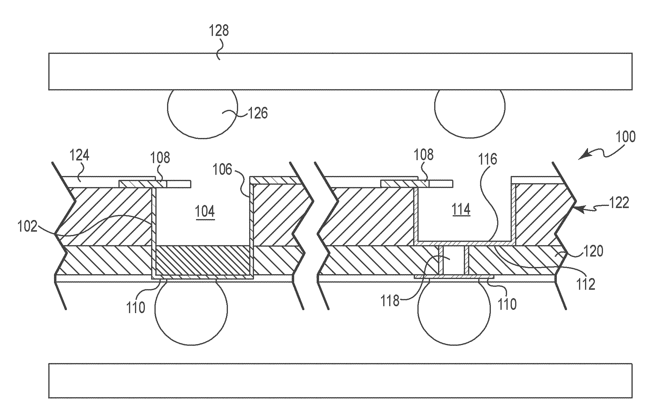
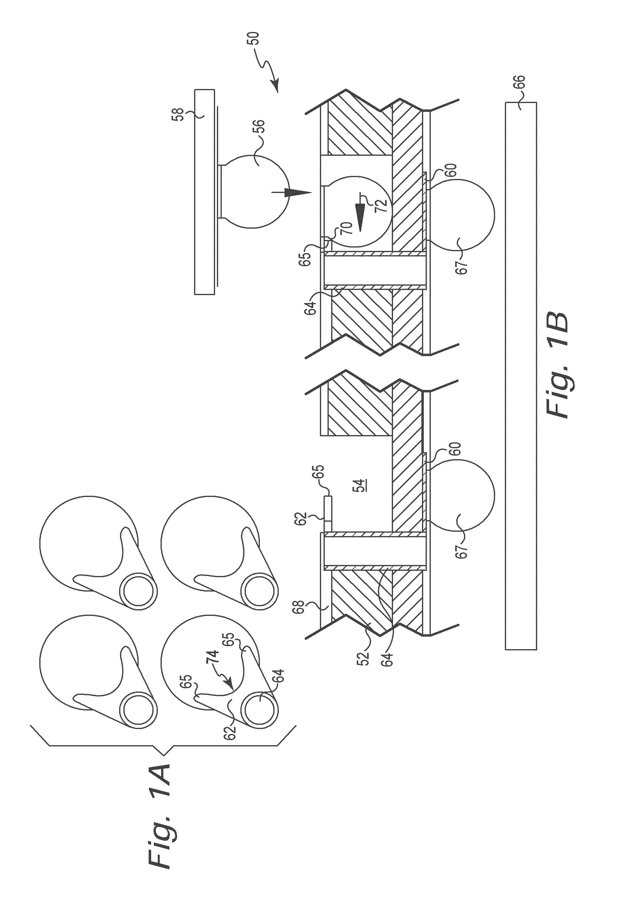
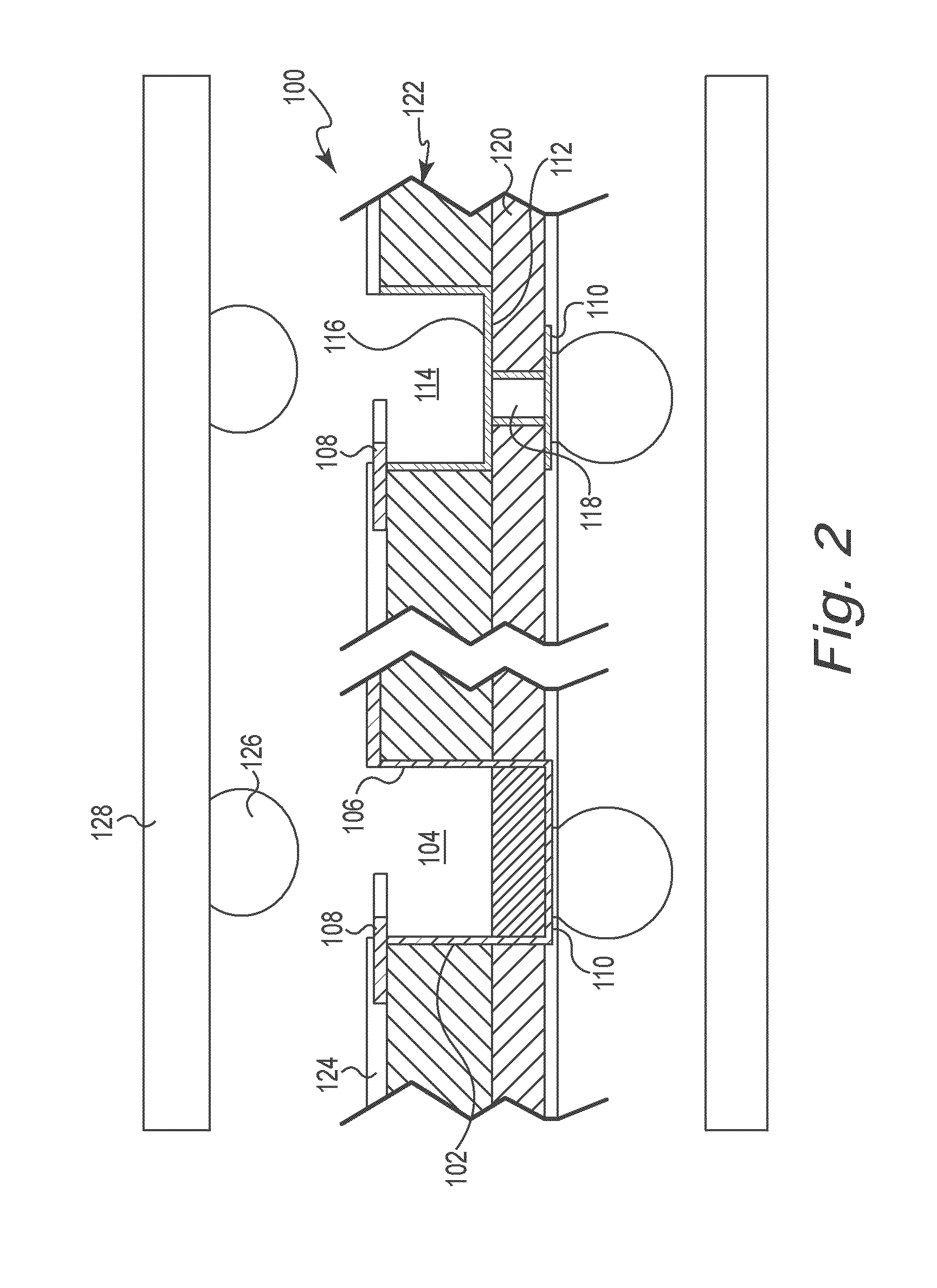
[0043]A high performance electrical interconnect according to the present disclosure may permit fine contact-to-contact spacing (pitch) on the order of less than 1.0 mm pitch, and more preferably a pitch of less than about 0.7 millimeter, and most preferably a pitch of less than about 0.4 millimeter. Such fine pitch high performance electrical interconnects are especially useful for communications, wireless, and memory devices.

[0044]The present high performance electrical interconnect can be configured as a low cost, high signal performance interconnect assembly, which has a low profile that is particularly useful for desktop and mobile PC applications. IC devices can be installed and uninstalled without the need to reflow solder. The solder-free electrical connection of the IC devices is environmentally friendly.

[0045]FIGS. 1A and 1B are top and cross-sectional views of a surface mount electrical interconnect 50 in accordance with an embodiment of the present disclosure. Socket sub...


PUM

PropertyMeasurementUnit
thickaaaaaaaaaa
aspect ratioaaaaaaaaaa

Abstract

A surface mount electrical interconnect adapted to provide an interface between solder balls on a BGA device and a PCB. A socket substrate is provided with a first surface, a second surface, and a plurality of openings sized and configured to receive the solder balls on the BGA device. A plurality of electrically conductive contact tabs are attached to the socket substrate so that contact tips on the contact tabs extend into the openings. The contact tips electrically couple with the BGA device when the solder balls are positioned in the openings. Vias electrically couple the contact tabs to contact pads located proximate the second surface of the socket substrate. Solder balls are bonded to the contact pads to electrically and mechanically couple the electrical interconnect to the PCB.

Description

RELATED APPLICATIONS[0001]This application claims the benefit of U.S. Provisional Application No. 61 / 452,875, filed Mar. 15, 2011, the disclosure of which is hereby incorporated by reference.[0002]This application is a continuation-in-part of U.S. patent application Ser. No. 13 / 266,573, titled COMPLIANT PRINTED CIRCUIT AREA ARRAY SEMICONDUCTOR DEVICE PACKAGE, filed Oct. 27, 2011, which is a national stage application under 35 U.S.C. §371 of International Application No. PCT / US2010 / 036363, titled COMPLIANT PRINTED CIRCUIT AREA ARRAY SEMICONDUCTOR DEVICE PACKAGE, filed May 27, 2010, which claims priority to U.S. Provisional Application No. 61 / 183,411, filed Jun. 2, 2009, all of which are hereby incorporated by reference in their entireties.[0003]This application is a continuation-in-part of U.S. patent application Ser. No. 13 / 320,285, titled COMPLIANT PRINTED FLEXIBLE CIRCUIT, filed Nov. 14, 2011, which is a national stage application under 35 U.S.C. §371 of International Application ...

Claims


Application Information

Patent Timeline
Patent Type & Authority Applications(United States)
IPC IPC(8): H01R12/71H05K3/00H05K3/34H01C17/06H01P11/00H01R43/16H01G4/00
CPCH01C1/14Y10T29/49099H01R12/523H01R12/7082H05K1/0231H05K1/141H05K3/3436H05K3/4038H05K3/4092H05K7/1069H05K7/1092H05K2201/049Y10T29/43Y10T29/49016Y10T29/49155Y10T29/4913Y10T29/49222H01G4/228
Inventor RATHBURN, JAMES
Owner HSIO TECH
Why Eureka
Try Eureka