Light-emitting device and method of manufacturing the same

a technology of light-emitting devices and manufacturing methods, applied in semiconductor/solid-state device manufacturing, semiconductor devices, electrical equipment, etc., can solve problems such as high failure rates, and achieve the effect of reducing electrical conduction and simplifying fabrication processes

Inactive Publication Date: 2012-10-04
SAMSUNG ELECTRONICS CO LTD
View PDF12 Cites 18 Cited by
  • Summary
  • Abstract
  • Description
  • Claims
  • Application Information

AI Technical Summary

Benefits of technology

[0009]Provided are a light-emitting device and a method of manufacturing the same, which simplify fabrication processes and reduce electrical conduction between electrode materials having opposite polarities by allowing the electrode materials to pass through a deposited insulating material.

Problems solved by technology

This may cause misalignment, resulting in a high failure rate.

Method used


Image

  • Light-emitting device and method of manufacturing the same
  • Light-emitting device and method of manufacturing the same
  • Light-emitting device and method of manufacturing the same

Examples


Embodiment Construction

[0018]Reference will now be made in detail to embodiments, examples of which are illustrated in the accompanying drawings, wherein like reference numerals refer to like elements throughout. In this regard, the present embodiments may have different forms and should not be construed as being limited to the descriptions set forth herein. Accordingly, the embodiments are merely described below, by referring to the figures, to explain aspects of the present description.

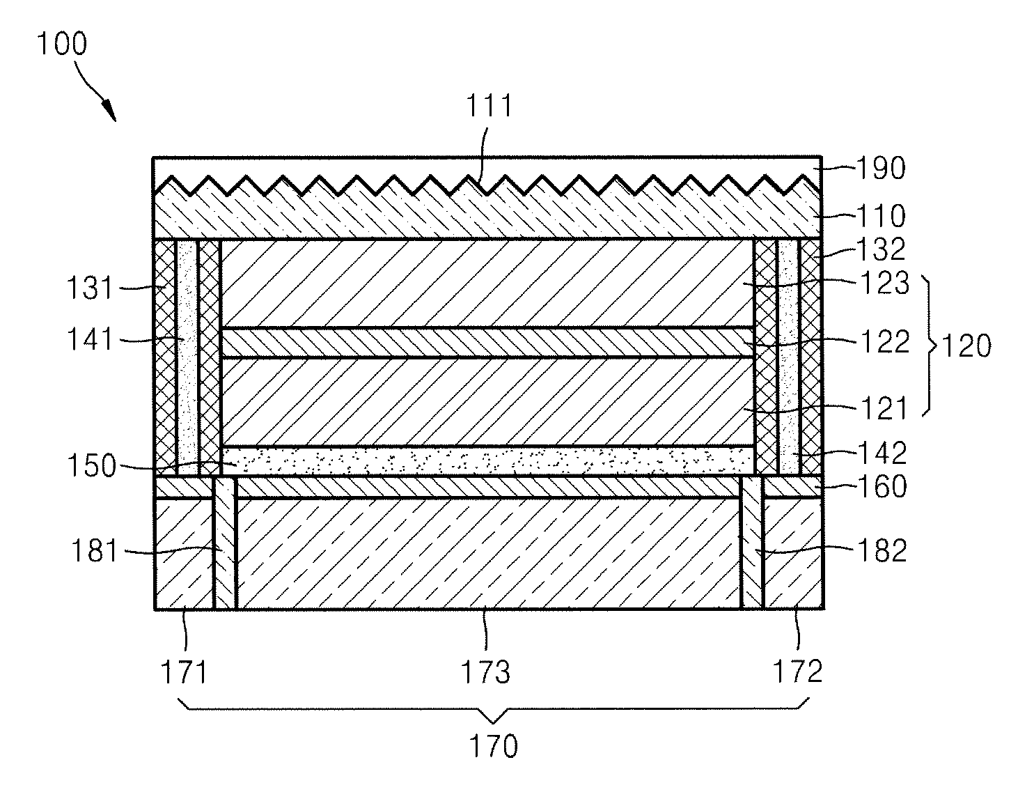
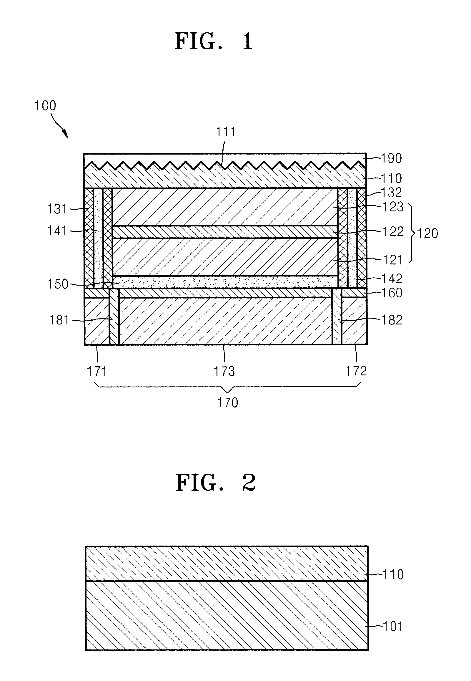
[0019]FIG. 1 is a cross-sectional view of a light-emitting device 100 according to an embodiment of the present invention.

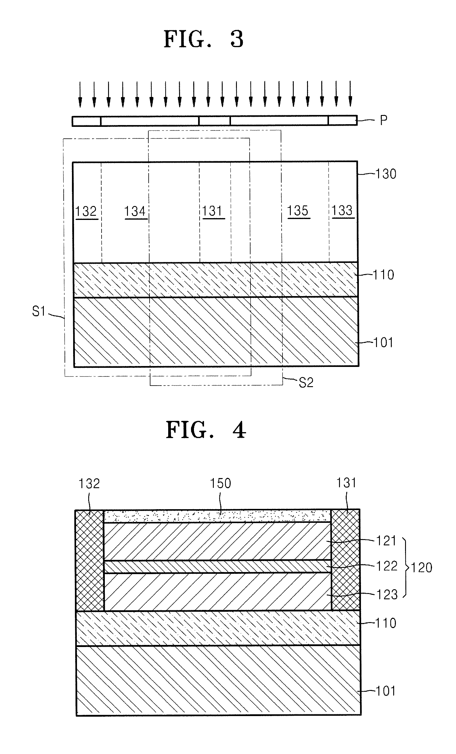
[0020]Referring to FIG. 1, the light-emitting device 100 according to the present embodiment includes a compound semiconductor structure 120, insulation walls 131 and 132 formed at either side of the compound semiconductor structure 120, and an electrode structure.

[0021]The compound semiconductor structure 120 includes a P-type compound semiconductor layer 121 grown on a predetermined substrate (101 in...


PUM


Abstract

A light-emitting device and a method of manufacturing the same are provided. The light-emitting device includes a compound semiconductor structure having a first N-type compound semiconductor layer, an active layer, and a P-type compound semiconductor layer, a P-type electrode layer that is disposed on the P-type compound semiconductor layer and electrically connects with the P-type compound semiconductor layer, a plurality of insulation walls disposed at two sides of the compound semiconductor structure and the P-type electrode layer, a plurality of N-type electrode layers penetrating the plurality of insulation walls, and a conductive substrate on which a plurality of N-type electrode connecting layers respectively corresponding to a plurality of N-type electrode layers are separated from a P-type electrode connecting layer corresponding to the P-type electrode layer.

Description

CROSS-REFERENCE TO RELATED APPLICATIONS[0001]This application claims the benefit of Korean Patent Application No. 10-2011-0029029, filed on Mar. 30, 2011, in the Korean Intellectual Property Office, the disclosure of is are incorporated herein in its entirety by reference.BACKGROUND[0002]1. Field[0003]The present disclosure relates to a light-emitting device and a method of manufacturing the same.[0004]2. Description of the Related Art[0005]A light-emitting device such as a light-emitting diode (LED) is used as a semiconductor light source with a pn junction of compound semiconductors and emits different light colors.[0006]For example, a nitride-based LED made of group III-V compounds such as gallium nitride (GaN), indium nitride (InN), and aluminum nitride (AlN) may be widely used as a light-emitting device that emits short-wavelength light (ultraviolet light and green light), and in particular, blue light. Light-emitting devices provide a long lifespan, a compact and lightweight d...

Claims


Application Information

Patent Timeline
Patent Type & Authority Applications(United States)
IPC IPC(8): H01L33/06H01L33/50
CPCH01L33/0079H01L33/20H01L33/382H01L2933/0016H01L33/44H01L33/505H01L33/385H01L33/007H01L33/0075H01L33/22H01L33/62H01L33/0093
Inventor PAEK, HO-SUNKIM, HAK-HWANOH, SUNG-KYONG
Owner SAMSUNG ELECTRONICS CO LTD
Why Eureka
Try Eureka