Light emitting diode device and producing method thereof

a technology of light-emitting diodes and producing methods, which is applied in the manufacture of semiconductor/solid-state devices, semiconductor devices, electrical devices, etc., can solve the problems of uneven white light emission of white light-emitting devices, non-uniform thickness of phosphor layers, and non-uniform efficiency of wavelength conversion in phosphor layers, etc., to achieve easy formation, short time, and suppress the effect of increasing production costs

Active Publication Date: 2012-10-04
EPISTAR CORP
View PDF3 Cites 13 Cited by
  • Summary
  • Abstract
  • Description
  • Claims
  • Application Information

AI Technical Summary

Benefits of technology

[0020]In the method for producing the light emitting diode device of the present invention, the phosphor layer in a sheet state is formed, so that the uniform phosphor layer can be reliably formed. Therefore, a uniform wavelength conversion can be achieved in the phosphor layer. As a result, the light emitting diode device of the present invention obtained by the method for producing the light emitting diode device of the present invention can emit uniform white light.
[0021]In the method for producing the light emitting diode device of the present invention, the phosphor layer, which is formed in a sheet state in advance, is formed, so that the phosphor layer can be easily formed in a short time. Therefore, an increase in the production costs can be suppressed.
[0022]In addition, in the method for producing the light emitting diode device of the present invention, the encapsulating resin layer that contains the light reflecting component is formed so as to cover the light semiconductor layer, so that light emitted from the light semiconductor layer is reflected by the light reflecting component of the encapsulating resin layer before being absorbed by another member. Therefore, the extraction efficiency of the light can be improved.
[0023]Furthermore, in the light emitting diode device of the present invention obtained by the method for producing the light emitting diode device of the present invention, the phosphor layer is formed at the other surface in the thickness direction of the light semiconductor layer, so that heat of the light semiconductor layer can be dissipated toward the other side in the thickness direction via the phosphor layer. Therefore, a reduction in the luminous efficiency of the light semiconductor layer can be prevented.
[0024]In the method for producing the light emitting diode device of the present invention, the light semiconductor layer is flip-chip mounted on the base board, so that the brightness can be improved and the extraction efficiency can be further improved.

Problems solved by technology

However, the phosphor layer in Japanese Unexamined Patent Publication No. 2005-191420 is a region defined according to a difference in concentration of the phosphor that is produced by a spontaneous precipitation of the phosphor in the mixture, so that a thickness of the phosphor layer easily becomes non-uniform.
In that case, there is a disadvantage that efficiency of the wavelength conversion in the phosphor layer becomes non-uniform and the white light emitting device emits uneven white light.
In addition, it is necessary to control the hours strictly, so that a production process becomes complicated.
As a result, there is a disadvantage that production costs are increased.
In addition, there is also a disadvantage that the semiconductor light emitting element is spaced apart from the reflecting frame portion, so that a part of the light emitted from the semiconductor light emitting element toward the side is absorbed in the encapsulating portion before being reflected at the reflecting frame portion and therefore, extraction efficiency of the light is reduced.
Thus, there is a disadvantage that a heat dissipation of the semiconductor light emitting element at the time of the emission becomes insufficient and as a result, luminous efficiency of the semiconductor light emitting element is reduced.

Method used


Image

  • Light emitting diode device and producing method thereof
  • Light emitting diode device and producing method thereof
  • Light emitting diode device and producing method thereof

Examples


example 1

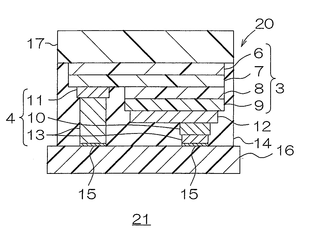
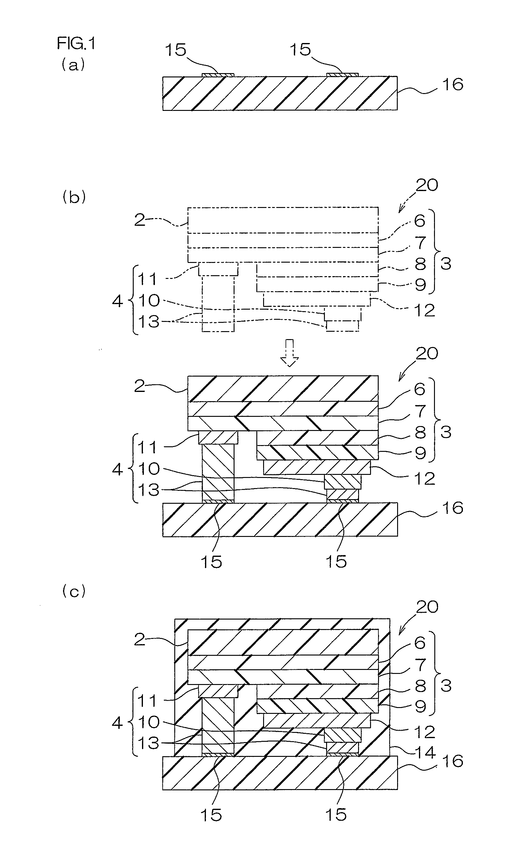
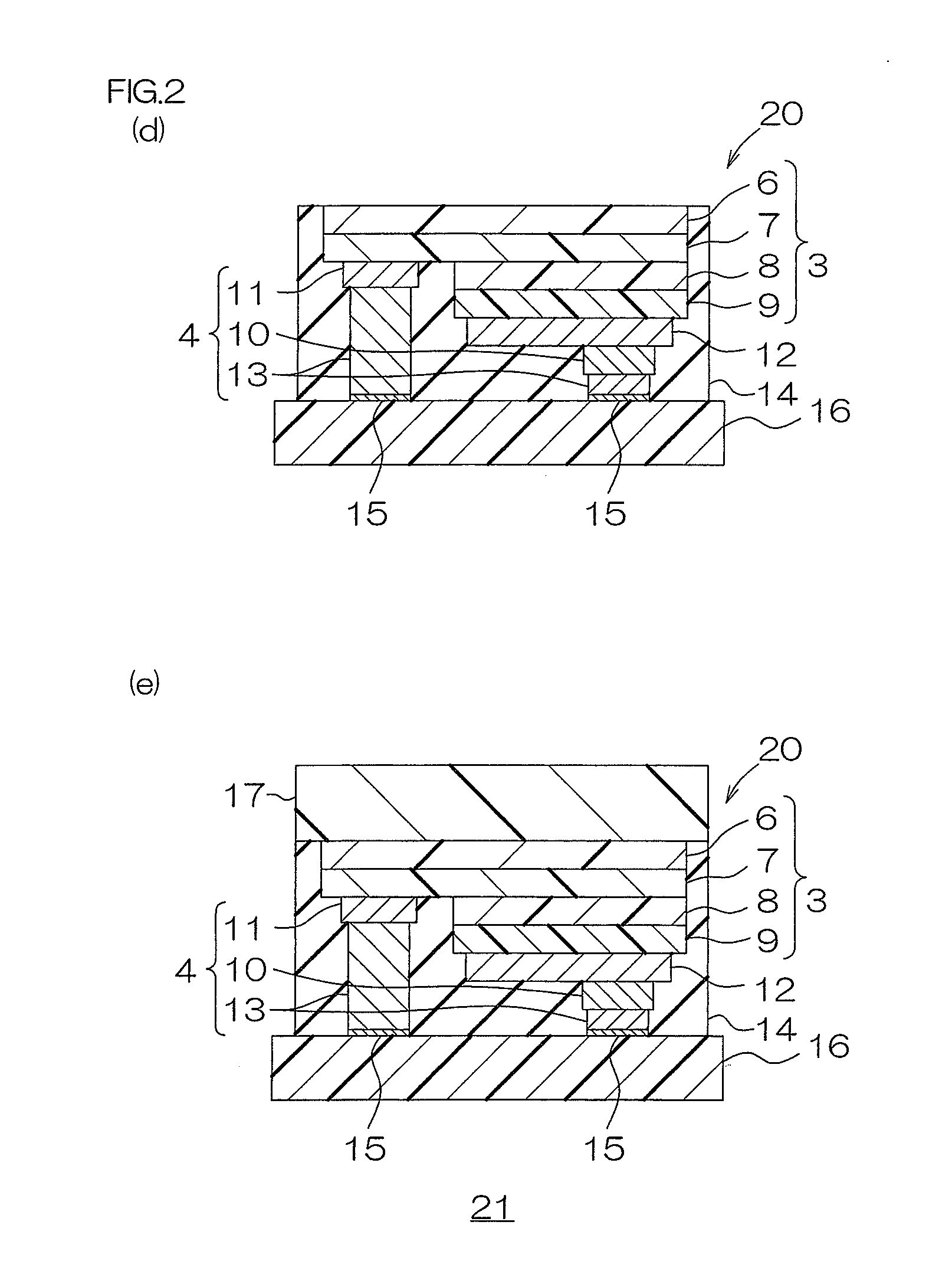
[0162]A base board in which a conductive layer including a terminal made of copper, nickel, and gold was laminated on the upper surface of an insulating board made of sapphire (Al2O3), having a thickness of 1 mm was prepared (ref: FIG. 1(a)).

[0163]A supporting board made of sapphire having a thickness of 450 μm was prepared (ref: FIG. 3). Subsequently, by an epitaxial growth method, a buffer layer made of GaN having a thickness of 30 nm, an N-type semiconductor layer made of N-type GaN (n-GaN:Si, hereinafter shown in the same manner) obtained by doping Si having a thickness of 5 μm, a light emitting layer made of InGaN having a thickness of 120 nm, and a P-type semiconductor layer made of p-GaN:Mg having a thickness of 50 nm were sequentially formed on the supporting board in the above-described pattern (ref: FIG. 3).

[0164]Next, an electrode portion was formed on the upper surface of a light semiconductor layer so as to be connected thereto by a patterning method (ref: FIG. 3).

[0165...


PUM


Abstract

A method for producing a light emitting diode device includes the steps of preparing a base board; allowing a light semiconductor layer where an electrode portion is provided at one side in a thickness direction to be disposed in opposed relation to the base board, and the electrode portion to be electrically connected to a terminal, so that the light semiconductor layer is flip-chip mounted on the base board; forming an encapsulating resin layer containing a light reflecting component at the other side of the base board so as to cover the light semiconductor layer and the electrode portion; removing the other side portion of the encapsulating resin layer so as to expose the light semiconductor layer; and forming a phosphor layer formed in a sheet state so as to be in contact with the other surface of the light semiconductor layer.

Description

CROSS-REFERENCE TO RELATED APPLICATION[0001]The present application claims priority from Japanese Patent Applications No. 2011-069768 filed on Mar. 28, 2011 and No. 2011-081854 filed on Apr. 1, 2011, the contents of which are hereby incorporated by reference into this application.BACKGROUND OF THE INVENTION[0002]1. Field of the Invention[0003]The present invention relates to a light emitting diode device and a producing method thereof, to be specific, to a producing method of a light emitting diode device and a light emitting diode device obtained by the method.[0004]2. Description of Related Art[0005]In recent years, as a light emitting device that is capable of emitting high-energy light, a white light emitting device has been known. In the white light emitting device, for example, a base board, an LED (light emitting diode) laminated thereon, emitting blue light, a phosphor layer that can convert the blue light into yellow light and covers the LED, and an encapsulating layer that...

Claims


Application Information

Patent Timeline
Patent Type & Authority Applications(United States)
IPC IPC(8): H01L33/50
CPCH01L33/46H01L33/505H01L2933/005H01L24/17H01L2224/16225H01L2924/12041H01L33/405H01L33/60H01L2924/00H01L2924/12042H01L2924/15787H01L2924/181H01L33/50H01L33/52
Inventor SATO, SATOSHIITO, HISATAKAOOYABU, YASUNARISHINBORI, YUKI
Owner EPISTAR CORP
Why Eureka
Try Eureka