Lithography system with differential interferometer module

a technology of differential interferometer and lithography system, which is applied in the field of lithography system, can solve the problems of displacement measurement error, displacement error negatively affecting alignment precision needed, focus error, etc., and achieve the effect of reducing system downtime and high positional accuracy

Active Publication Date: 2012-10-04
ASML NETHERLANDS BV
View PDF3 Cites 20 Cited by
  • Summary
  • Abstract
  • Description
  • Claims
  • Application Information

AI Technical Summary

Benefits of technology

[0043]In a system according to this embodiment an entire differential interferometer module may be mounted or replaced within the vacuum chamber, without having to align the beam splitter and / or beam combiner of the module. Downtime of the system is thus reduced.
[0044]In an embodiment said one or more interferometer module is mounted to said frame by means of a kinematic mount. Expansion of the frame and / or the module, for instance due to thermal expansion thereof, thus does not substantially affect the alignment of the module. Moreover, further calibration of the module once it has been mounted is no longer required as it may be mounted on the frame with high positional accuracy.

Problems solved by technology

A typical problem with interferometer based measurement systems is that small errors in the reflective surface of a mirror, for instance due to mirror unflatness and / or due to thermal expansion of the target carrier or optical column, result in displacement measurement errors due to Abbe and Cosine errors.
Displacement errors negatively affect alignment precision needed for instance for stitching or overlay of a pattern.
In such a systems errors in Rx and / or Ry of the projection lens optics lead to focus errors when projecting an image onto a target exposure surface.
This large number of interferometers increases complexity of the system and substantially increases downtime of the system needed for adjusting and / or replacing the interferometers.

Method used


Image

  • Lithography system with differential interferometer module
  • Lithography system with differential interferometer module
  • Lithography system with differential interferometer module

Examples


Embodiment Construction

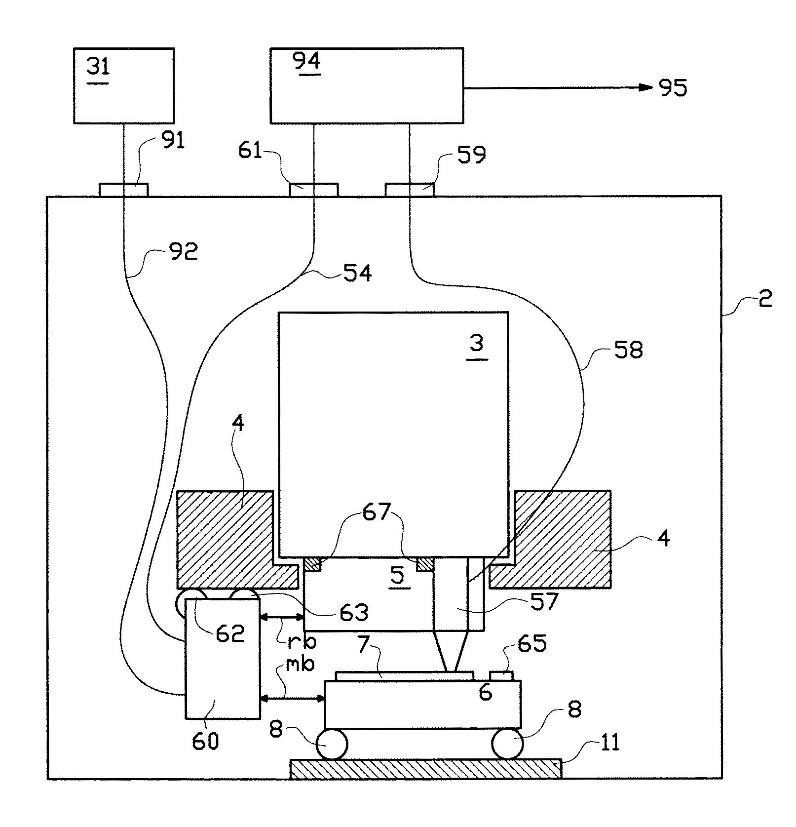
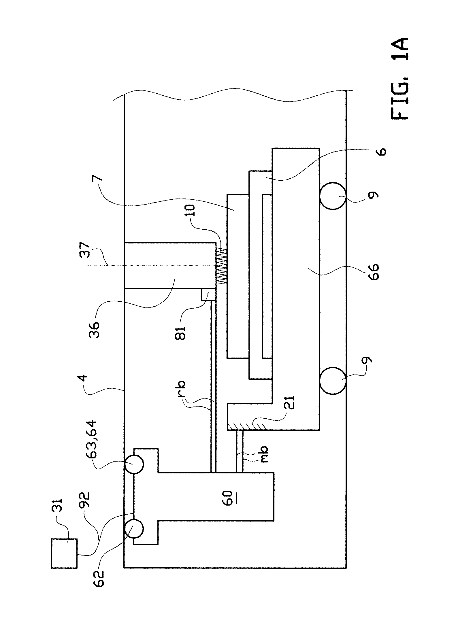
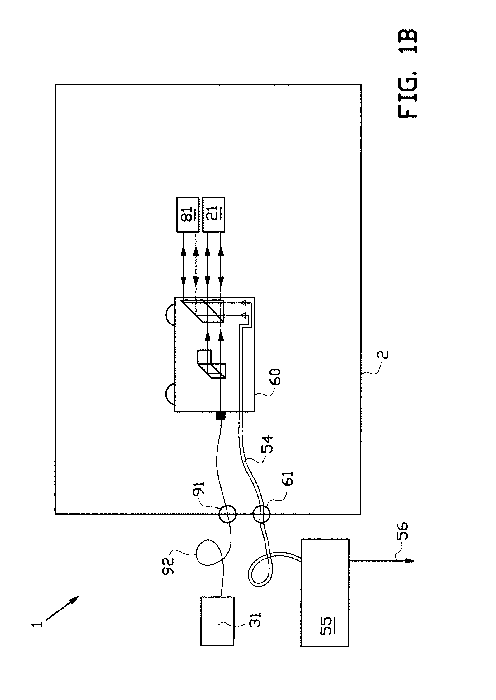
[0073]FIG. 1A shows a lithography system 1 according to the present invention. The system comprises a frame 4, to which an optical column 36 having an optical axis 37 is mounted. The optical column is adapted for projecting a plurality of exposure beamlets 10 onto a target 7. By selectively switching selected exposure beamlets on or of, an exposure surface of the target below the optical column may be patterned. The target is placed on a wafer table 6, which in turn is placed on a chuck 66 which is moveable with respect to the optical column 36 by means of a stage 9 on which the chuck 66 is placed. In the embodiment shown, the chuck, wafer table and stage form a target carrier for moving the target 7 relative to the optical column 36.

[0074]The chuck 66 comprises a first mirror 21, comprising a substantially planar surface at substantially the same level or height within the system as the target 7 or exposure surface thereof. The optical column comprises a second mirror 81, which com...


PUM


Abstract

The invention relates to a lithography system comprising an optical column, a moveable target carrier for displacing a target such as a wafer, and a differential interferometer module, wherein the interferometer module is adapted for emitting three reference beams towards a first mirror and three measurement beams towards a second mirror for determining a displacement between said first and second mirror. In a preferred embodiment the same module is adapted for measuring a relative rotation around two perpendicular axes as well. The present invention further relates to an interferometer module and method for measuring such a displacement and rotations.

Description

BACKGROUND[0001]The invention relates to a lithography system comprising an optical column, a moveable target carrier for displacing a target such as a wafer, and a differential interferometer, wherein the interferometer is adapted for measuring a displacement between a mirror provided on the optical column and a mirror provided on the target carrier. The present invention further relates to an interferometer module and method for measuring such a displacement.[0002]A typical problem with interferometer based measurement systems is that small errors in the reflective surface of a mirror, for instance due to mirror unflatness and / or due to thermal expansion of the target carrier or optical column, result in displacement measurement errors due to Abbe and Cosine errors. Displacement errors negatively affect alignment precision needed for instance for stitching or overlay of a pattern.[0003]Errors in Rz rotation of the optical column are especially a factor of importance in lithography...

Claims


Application Information

Patent Timeline
Patent Type & Authority Applications(United States)
IPC IPC(8): G03B27/42G01B9/02G01B11/14
CPCG03F7/70775H01J2237/30438G03F7/7085G03F7/70833G01B9/02011G01B9/02012G01B9/02027G02B27/283G03F7/70591H01L21/0274H01J2237/3175G01B9/02016G03F7/20G01B9/02007G01B9/02015
Inventor DE BOER, GUIDOOOMS, THOMAS ADRIAANVERGEER, NIELSCOUWELEERS, GODEFRIDUS CORNELIUS ANTONIUS
Owner ASML NETHERLANDS BV
Why Eureka
Try Eureka