Methods For Accessing DRAM Cells Using Separate Bit Line Control

a bit line control and access method technology, applied in the field of sense amplifiers, can solve the problems of up to 20-30% signal loss, the storage node voltage v/sub>sn/sub> of the pmos bit cell b>109/b> has not had enough time to reach the desired voltage of 0 volts, etc., and achieve the effect of improving the access tim

Active Publication Date: 2012-10-04
MOSYS INC
View PDF2 Cites 8 Cited by
  • Summary
  • Abstract
  • Description
  • Claims
  • Application Information

AI Technical Summary

Benefits of technology

[0019]This memory system allows for several improved methods for accessing the DRAM cells. In accordance with one embodiment, the first and second bit lines are initially driven to a pre-charge voltage. After the first and second bit lines are pre-charged, the first bit line is isolated from the pre-charge voltage, and a DRAM cell coupled to the...

Problems solved by technology

However, capacitive coupling between the bit lines BL and BL# undesirably causes the voltage on the reference bit line BL# to be pulled toward the voltage of the selected bit line BL (i.e., the voltage on the reference bit line BL# deviates from the pre-charged voltage of...

Method used


Image

  • Methods For Accessing DRAM Cells Using Separate Bit Line Control
  • Methods For Accessing DRAM Cells Using Separate Bit Line Control
  • Methods For Accessing DRAM Cells Using Separate Bit Line Control

Examples


Embodiment Construction

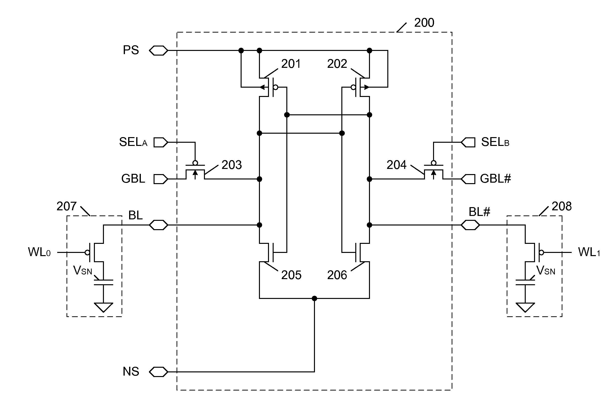
[0038]FIG. 2A is a circuit diagram of a six transistor (6T) sense amplifier circuit 200 and PMOS bit cells 207-208 in accordance with one embodiment of the present invention. Sense amplifier 200 includes PMOS transistors 201-204 and NMOS transistors 205-206, which are connected as illustrated. Transistors 201 and 205 are connected to form a first inverter, and transistors 202 and 206 are connected to form a second inverter. These two inverters are cross-coupled to form a latch circuit, which is coupled to complementary bit lines BL and BL#. Exemplary PMOS bit cells 207 and 208 are shown coupled to bit lines BL and BL#, respectively, for purposes of illustration. It is understood that a plurality of bit cells are typically connected to each of the bit lines BL and BL#, wherein each of the bit cells has a corresponding word line.

[0039]The source and body regions of PMOS transistors 201-202 are coupled to receive a control voltage PS. The source regions of NMOS transistors 205-206 are ...


PUM


Abstract

A memory system that includes a first bit line coupled to a first set of dynamic random access memory (DRAM) cells, a second (complementary) bit line coupled to a second set of DRAM cells, and a sense amplifier coupled to the first and second bit lines. The sense amplifier includes a pair of cross-coupled inverters (or a similar latching circuit) coupled between the first and second bit lines, as well as a first select transistor coupling the first bit line to a first global bit line, and a second select transistor coupling the second bit line to a second global bit line. The first and second select transistors are independently controlled, thereby enabling improved read and write access sequences to be implemented, whereby signal loss associated with bit line coupling is eliminated, ‘read bump’ conditions are eliminated, and late write conditions are eliminated.

Description

RELATED APPLICATIONS[0001]The present application is related to, and incorporates by reference, the following commonly owned, co-filed U.S. patent applications: Ser. No. 13 / ______ filed by Richard S. Roy and Dipak K. Sikdar on Mar. 31, 2011, entitled “Separate Pass Gate Controlled Sense Amplifier”.FIELD OF THE INVENTION[0002]The present invention relates to a sense amplifier for a dynamic random access memory (DRAM) cells.RELATED ART[0003]FIG. 1A is a circuit diagram of a conventional eight transistor (8T) DRAM sense amplifier 100, which is coupled to DRAM cells 109-110 having PMOS access transistors (PMOS bit cells). DRAM sense amplifier 100 includes PMOS transistors 101-102 and NMOS transistors 103-108, which are connected as illustrated. PMOS transistors 101-102 and NMOS transistors 103-104 form a cross-coupled latch, which is coupled to PMOS bit cells 109 and 110 by complementary bit lines BL and BL#, respectively. The source and body regions of PMOS transistors 101-102 are coup...

Claims


Application Information

Patent Timeline
IPC IPC(8): G11C7/12
CPCG11C11/4091G11C2207/005G11C11/4097
Inventor ROY, RICHARD S.SIKDAR, DIPAK K.
Owner MOSYS INC
Why Eureka
Try Eureka