Nanocone-based photovoltaic solar cells

a photovoltaic solar cell and nano-based technology, applied in the field of photovoltaic devices, can solve the problems of limited photoelectric conversion efficiency of these planar solar cells, the inability to control the thickness of these planar material layers, and the inability to collect charge carriers generated by the photons, etc., and achieve the effect of efficient charge collection

Inactive Publication Date: 2012-10-11
UT BATTELLE LLC
View PDF2 Cites 10 Cited by
  • Summary
  • Abstract
  • Description
  • Claims
  • Application Information

AI Technical Summary

Benefits of technology

[0004]A photovoltaic structure including a nanocone-based three-dimensional interdigitated p-n junction is provided in the present invention. The three-dimensional p-n junction is at the interface between n-type oxide semiconductor nanocones and a p-type semiconductor material that functions as a matrix either partially or fully embedding the nanocones. The nanocone-based three-dimensional p-n junction allows efficient minority carriers crossing across the p-n junction, and generates completely-depleted regions throughout the nanocones and the matrix around the nanocones for efficient charge collection. Further, the band gap energies of the both n-type and p-type semiconductor materials can be tuned to match the solar light spectrum by mixing related elements.
[0005]Additionally, the present invention provides methods of synthesizing Zn1-xCdxO nanocones on indium-tin-oxide and other solar-transparent substrates, methods of synthesizing CdTe and ZnTe p-type matrix between nanocones, and methods of minimizing interfacial defects using pulsed thermal processing (PTP). The value of x can be from 0 to 1, i.e., 0, 1, or any value therebetween.
[0006]The nanocone-based photovoltaic structure of the present invention can be formed by first growing an array of vertically aligned oxide semiconductor nanocones on a transparent conductive oxide (TCO) substrate in the ambient of a lateral growth control agent. The lateral growth control agent allows growth at the ledges located at the periphery of the uppermost surface of a oxide semiconductor frustum (a cone with its apex cut off by a plane parallel to its base) less than at the upper surface of the oxide semiconductor frustum, thereby providing a taper to the sidewalls of the oxide semiconductor frustum until the oxide semiconductor nanocones are completed. Vertical alignment of the nanocones is ensured by depositing aluminum-doped ZnO film prior to the nanocone synthesis. A p-type CdTe semiconductor material can be conformally deposited on the array of oxide semiconductor nanocones, and effectively activated by an anneal that can be performed in a CdCl2 solution or in CdCl2 vapor. The solar cell structure has a depletion zone that encompasses the entirety of the oxide semiconductor nanocones and the p-type semiconductor material embedding the oxide semiconductor nanocones. An electrical field distribution that is inherently generated by the oxide semiconductor nanocones facilitate (1) photon-generated minority charge carriers to cross over the p-n junction in both the embedding CdTe material and in the oxide semiconductor nanocones and (2) majority carriers, either originating from photo-generation or from the crossover, to move to their respective electrodes.

Problems solved by technology

A conflict arises in controlling the thicknesses of these planar material layers.
If the planar layers are thick, charge carriers generated by the photons cannot get collected because they are trapped by defects existed in these thick layers.
Therefore photo-electrical conversion efficiency is limited for these planar solar cells.

Method used


Image

  • Nanocone-based photovoltaic solar cells
  • Nanocone-based photovoltaic solar cells
  • Nanocone-based photovoltaic solar cells

Examples


Embodiment Construction

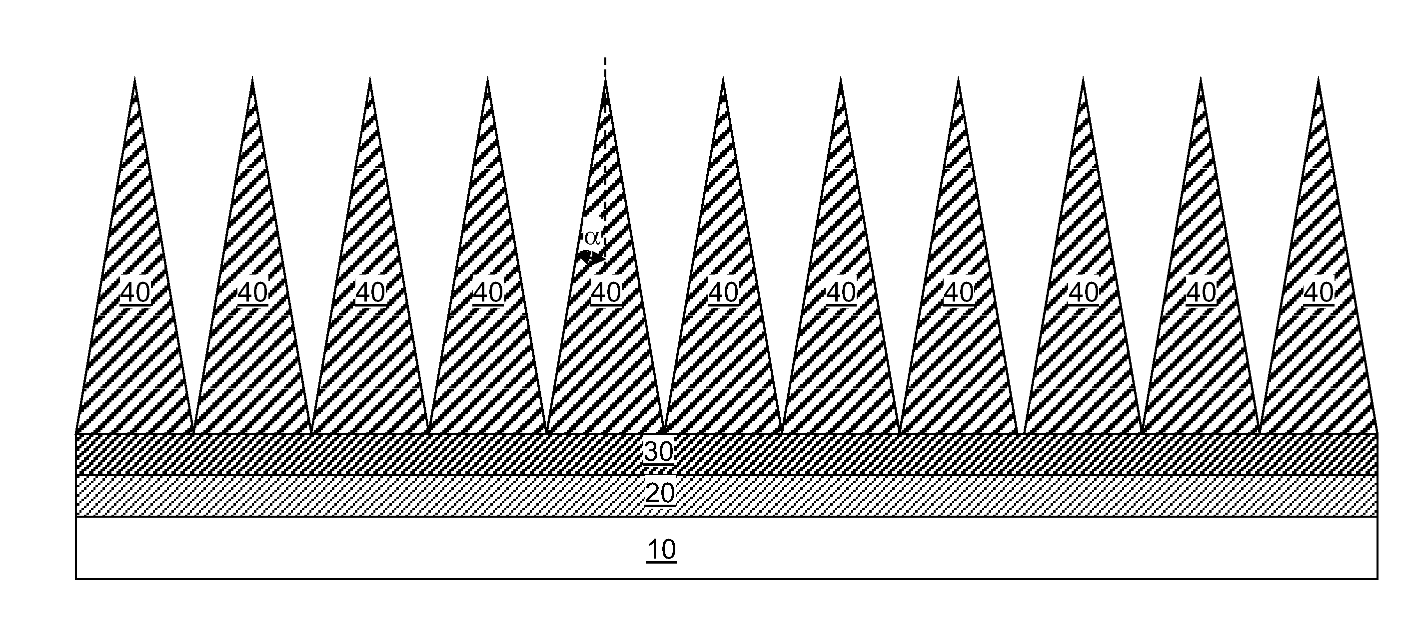
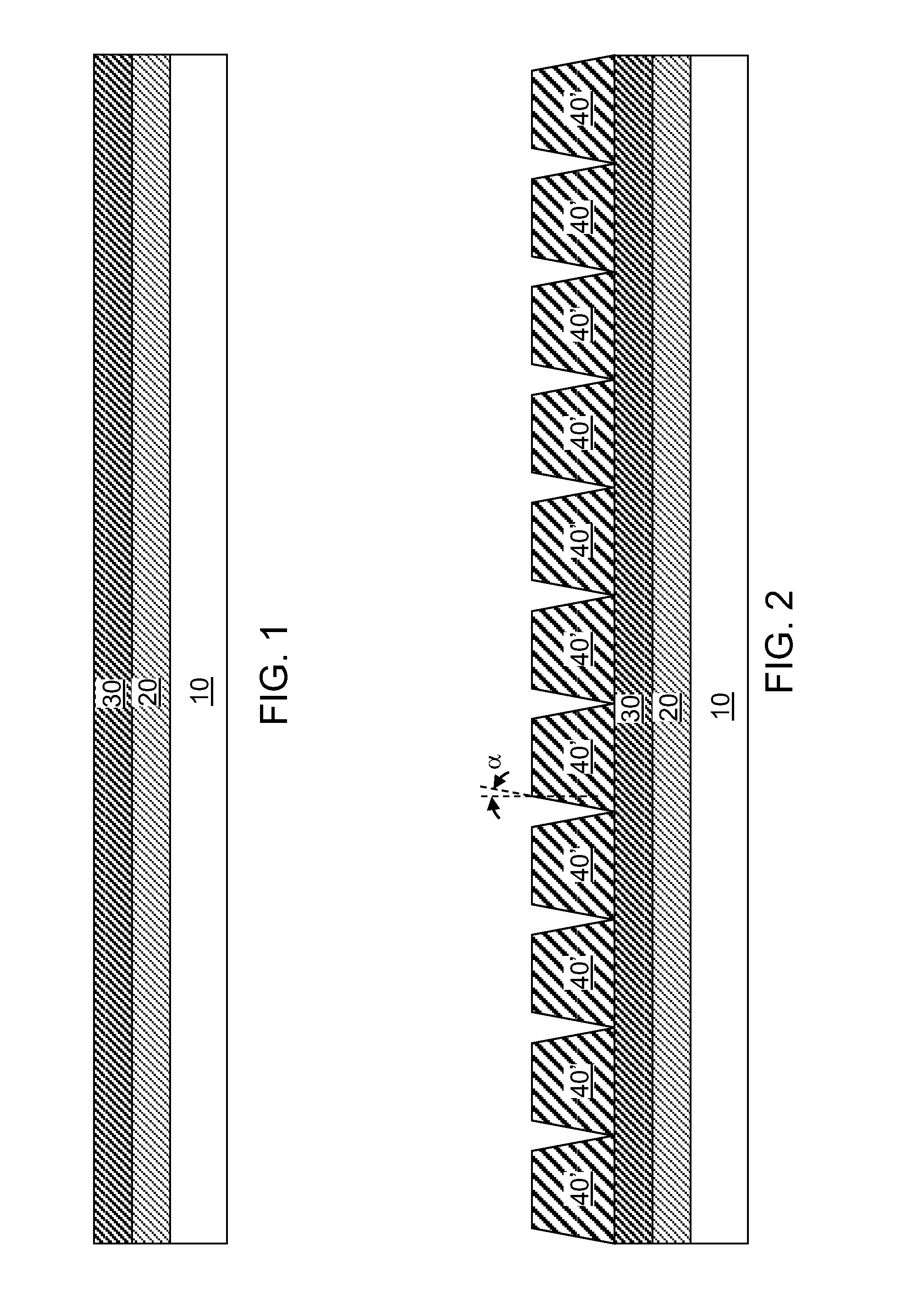
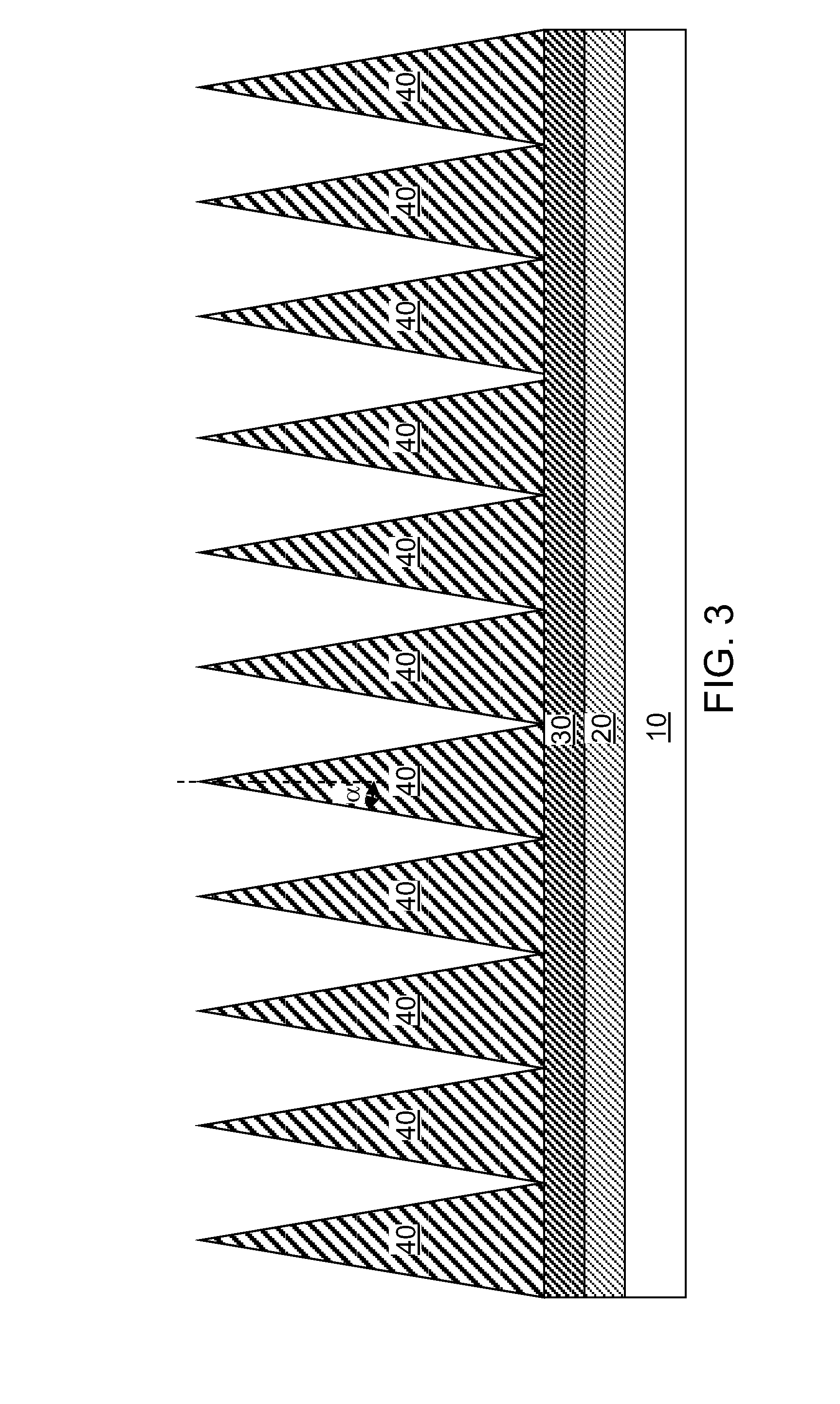
[0023]As stated above, the present invention relates to a photovoltaic device including a nanocone structure, and methods of manufacturing the same, which are now described in detail with accompanying figures. It is noted that like and corresponding elements mentioned herein and illustrated in the drawings are referred to by like reference numerals. It is also noted that proportions of various elements in the accompanying figures are not drawn to scale to enable clear illustration of elements having smaller dimensions relative to other elements having larger dimensions.

[0024]As used herein, a “transparent conductive oxide (TCO) substrate” refers to any electrically conductive substrate that is transmissive, allowing solar radiation to pass through, while providing an electrode contact for a device thereupon.

[0025]As used herein, a “depleted region,” or a “depleted junction region” refers to a semiconductor region in which static electric field is present in the absence of illuminati...


PUM


Abstract

A photovoltaic structure including a nanocone-based three-dimensional interdigitated p-n junction is provided in the present invention. The three-dimensional p-n junction is at the interface between n-type oxide semiconductor nanocones and a p-type semiconductor material that functions as a matrix embedding the nanocones. The nanocone-based three-dimensional p-n junction allows efficient minority carriers being extracted from photo-absorber and crossing across the p-n junction, and generates completely-depleted regions throughout the nanocones and the matrix around the nanocones for efficient charge collection. Further, the bandgap energies of the p-doped semiconductor material can be tuned to match the solar light spectrum by mixing related elements. Further, the high temperature pulses can be used to remove defects in the junction interfaces and sintering nanoparticle matrix.

Description

STATEMENT REGARDING FEDERALLY SPONSORED RESEARCH OR DEVELOPMENT[0001]This invention was made with government support under Contract No. DE-AC05-00OR22725 awarded by the U.S. Department of Energy. The government has certain rights in this invention.FIELD OF THE INVENTION[0002]The present invention relates to a photovoltaic device, and particularly to a photovoltaic device including a nanocone structure, and methods of manufacturing the same.BACKGROUND OF THE INVENTION[0003]Currently, all commercial photovoltaic structures employ planar structures. A conflict arises in controlling the thicknesses of these planar material layers. If the planar layers are thin, solar light cannot be completely absorbed by the layers. If the planar layers are thick, charge carriers generated by the photons cannot get collected because they are trapped by defects existed in these thick layers. Therefore photo-electrical conversion efficiency is limited for these planar solar cells.SUMMARY OF THE INVENTION...

Claims


Application Information

Patent Timeline
Patent Type & Authority Applications(United States)
IPC IPC(8): H01L31/06H01L31/0336
CPCY02E10/543H01L31/03529H01L31/1836H01L31/073H01L31/1828H01L31/03925
Inventor XU, JUNLEE, SANG HYUNSMITH, DAVID BARTONZHANG, XIAOGUANGDUTY, CHAD E.
Owner UT BATTELLE LLC
Why Eureka
Try Eureka