Semiconductor integrated circuit device

Active Publication Date: 2012-10-11
SOCIONEXT INC
View PDF10 Cites 2 Cited by
  • Summary
  • Abstract
  • Description
  • Claims
  • Application Information

AI Technical Summary

Benefits of technology

[0021]According to the foregoing aspect, the first capacitive element, which includes a transistor having a decoupling capacity, is formed under the first power supply wiring and is located on the portion at the second power supply wiring side and the portion at the third power supply wiring side. In other words, the first capacitive element is formed such that it extends across the first power supply wiring. This structure allows obtaining a greater gate width of the tra

Problems solved by technology

However, the higher frequency invites the greater noises, and the lower operating voltage invites the weaker resistance to noises, so that the LSI of nowadays tends to encounter a malfunction

Method used


Image

  • Semiconductor integrated circuit device
  • Semiconductor integrated circuit device
  • Semiconductor integrated circuit device

Examples


embodiment 1

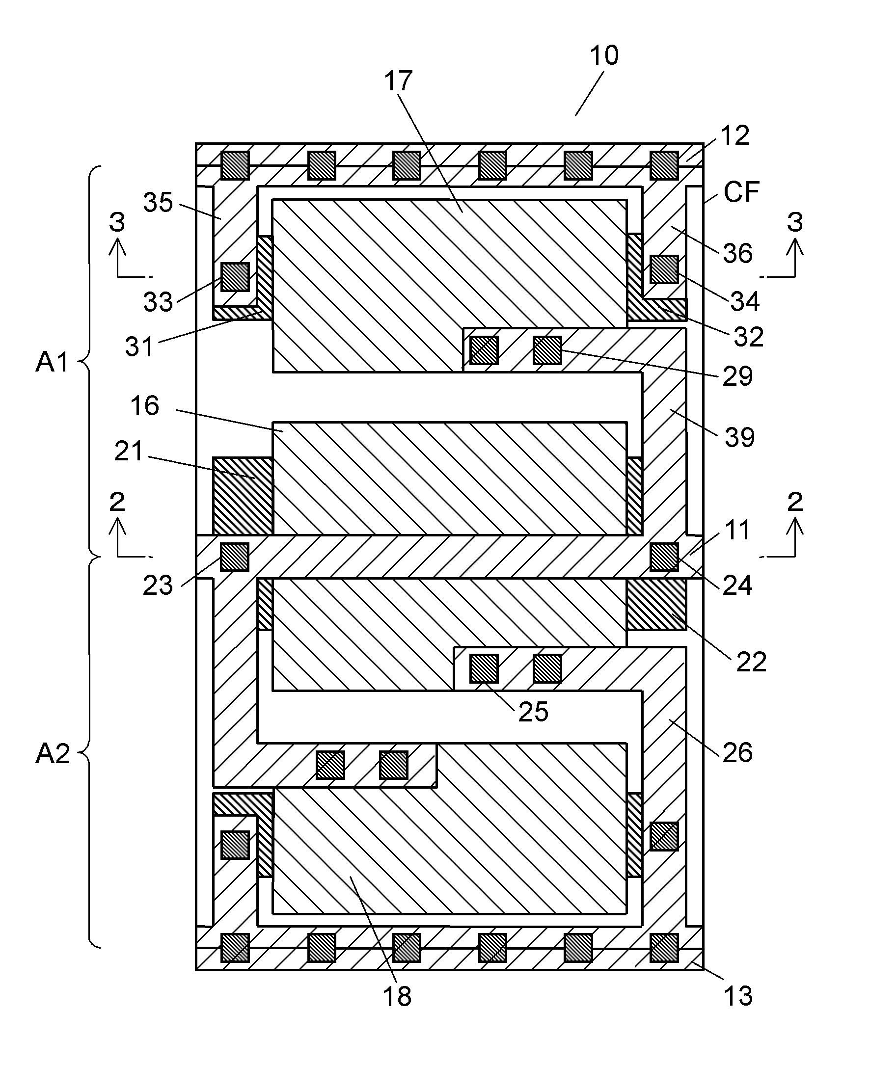
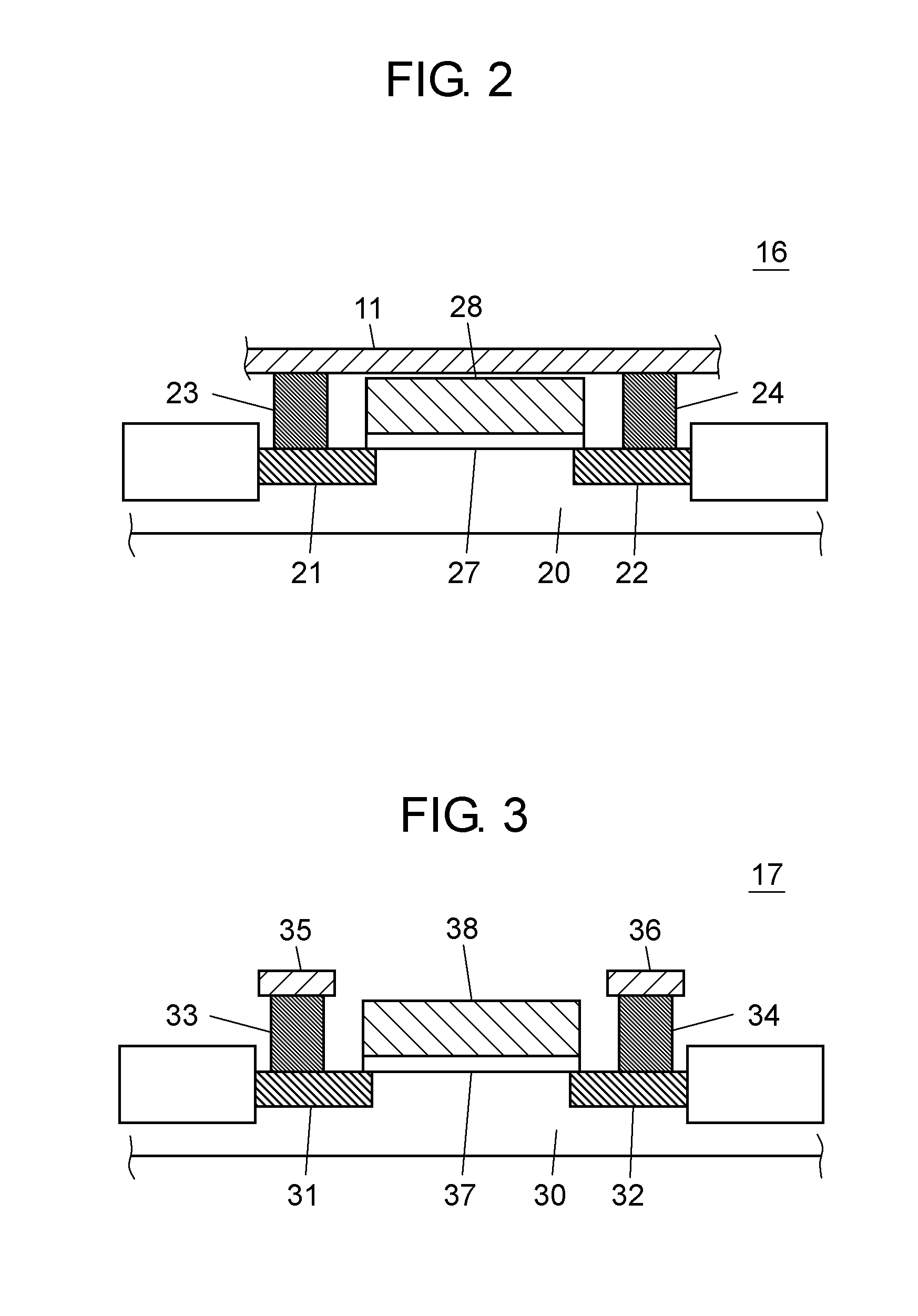
[0038]FIG. 1 is a plan view illustrating a layout of a capacity cell in accordance with the first embodiment. The capacity cell shown in FIG. 1 and other cells are disposed for forming a semiconductor integrated circuit device in accordance with the first embodiment. In this embodiment, assume that respective metal wirings are provided to a first layer.

[0039]In FIG. 1, capacity cell 10 is formed in cell frame CF having a double-height structure. Cell frame CF is formed by layering two circuit portions A1 and A2, along a vertical direction in FIG. 1. Each of the two circuit portions A1 and A2 has a single height structure. The double height structure shown in FIG. 1 is formed by layering circuit portions A1 and A2, both having the single height structure, in the vertical direction of FIG. 1 with an N-well shared with each other. Not to mention, a circuit portion with single height structure is disposed adjacently to another one with a P-well shared with each other, thereby forming a ...

embodiment 2

[0061]Fine processes of process rule 65 nm and onward encounter weaker noise resistance caused by a thinner film of gate oxide, so that a probability of breakdown of the gate oxide film increases. On the other hand, a power-supply wiring or a ground wiring designed to have lower impedance tends to carry noises. Considering these facts, the foregoing problem of the breakdown of the gate oxide film is a serious concern about the structure shown in FIG. 1 where the gate terminal is directly connected with the power-supply wiring or the ground wiring.

[0062]It is thus desirable that a circuit for providing a stable voltage be disposed between the gate terminal and the power supply wiring or the ground wiring in order to prevent noises exceeding a rated withstanding voltage from entering the gate terminal so that supply voltage VDD and ground voltage VSS can be steadily supplied to the gate terminal. This circuit for supplying a voltage steadily is referred to as a TIE portion. The TIE po...

embodiment 3

[0070]FIG. 6 is a plan view illustrating a layout of a capacity cell in accordance with the third embodiment. The structure shown in FIG. 6 is similar to that shown in FIG. 4 except the shapes of gate patterns of second and third capacitive elements 17A and 18A. Structural elements similar to those in FIG. 4 have the same reference marks, and detailed descriptions thereof are omitted here.

[0071]Capacity cell 60 shown in FIG. 6 includes second capacitive element 17A formed of a transistor of which gate pattern has multiple projections 61 projecting toward metal wiring 12 along the vertical direction in FIG. 6. Respective projections 61 are placed at intervals equal to each other, and have widths equal to each other along the lateral direction in FIG. 6. The tips of respective projections 61 are positioned vertically in FIG. 6 at the same location and aligned laterally. In a similar way, a transistor forming third capacitive element 18A has multiple projections 62 projecting toward me...


PUM


Abstract

A layout for a semiconductor integrated circuit device can maintain a sufficient capacitance of a capacity cell even when a height of the cell is lowered. In this layout, power supply wiring extending along a first direction supplies a first supply voltage, power supply wiring and power supply wiring extending in parallel with the power-supply wiring supply a second and a third supply voltages respectively. Capacitive element is formed of a transistor that receives the first supply voltage at its source and drain, and receives the second or the third supply voltages at its gate. Capacitive element is disposed under power supply wiring such that it strides over a portion at power supply wiring side and a portion at power supply wiring side.

Description

BACKGROUND[0001]1. Technical Field[0002]The present invention relates to a layout of a semiconductor integrated circuit device having a decoupling capacity for preventing a malfunction caused by power supply noises.[0003]2. Background Art[0004]A conventional semiconductor device has achieved a variety of circuit units, which implement desirable functions, through the placement, at will, of transistors having various widths and lengths. The circuit unit is referred to as a cell, and the cells are combined and wired together to form an LSI (large scale integration).[0005]In recent years, the LSI has undergone a rapid progress in a finer micro-process and a higher dense integration. This market trend has entailed a lower operating voltage and a higher operating frequency. For instance, the LSI thus requires performance such as a process rule of 0.1 μm or less, an operating voltage of 1.2V or less, and an operating frequency of several hundreds MHz or greater.[0006]However, the higher f...

Claims


Application Information

Patent Timeline
IPC IPC(8): H03K3/01
CPCH01L23/642H01L27/0811H01L27/11807H01L29/66181H01L29/94H01L2924/0002H01L23/5286H01L2924/00
Inventor NAKANISHI, KAZUYUKI
Owner SOCIONEXT INC
Why Eureka
Try Eureka