Light trapping architecture for photovoltaic and photodector applications

a light trapping and photodetector technology, applied in the direction of instruments, optical elements, photoelectric discharge tubes, etc., can solve the problems of difficult and expensive production of efficient crystalline-based devices, low efficiency, and low efficiency of detection circuits, so as to increase the collection of light and high efficiency photoconversion

Active Publication Date: 2012-10-18
RGT UNIV OF MICHIGAN
View PDF7 Cites 12 Cited by
  • Summary
  • Abstract
  • Description
  • Claims
  • Application Information

AI Technical Summary

Benefits of technology

[0034]There is also disclosed a high efficiency photoconversion structure for trapping and converting incident light to electrical energy, optionally including an optical concentrator to increase the collection of light. Non-limiting examples of optical concentrators that can be used according to the present disclosure include conical parabolic and trough-shaped parabolic optical concentrators.
[0035]In one embodiment, there is disclosed a high efficiency photoconversion structure in which the incident light is admitted generally perpendicular to the planes of the photosensitive material layers. In another embodiment, there is disclosed a high efficiency photoconversion structure in which the incident light is admitted generally parallel to the planes of the photosensitive material layers.

Problems solved by technology

As a general rule, a photovoltaic cell provides power to a circuit, device or equipment, but does not provide a signal or current to control detection circuitry, or the output of information from the detection circuitry.
In contrast, a photodetector or photoconductor provides a signal or current to control detection circuitry, or the output of information from the detection circuitry but does not provide power to the circuitry, device or equipment.
However, efficient crystalline-based devices, especially of large surface area, are difficult and expensive to produce due to the problems inherent in producing large crystals without significant efficiency-degrading defects.
On the other hand, high efficiency amorphous silicon devices still suffer from problems with stability.
The maximum total power generated by a PV device is inherently incapable of exceeding the product, ISC×VOC.
Either of these outcomes is undesirable in a photosensitive optoelectronic device.
Such a process can be induced by the built-in electric field, but the efficiency at the electric fields typically found in organic devices (F˜106 V / cm) is low.
However, organic PV devices typically have relatively low quantum yield (the ratio of photons absorbed to carrier pairs generated, or electromagnetic radiation to electricity conversion efficiency), being on the order of 1% or less.
Generally, the absorption constant for a given photoconductive medium is not adjustable.
For certain photoconductive materials, e.g., 3,4,9,10 perylenetetracarboxylic-bis-benzimidazole (PTCBI), or copper phthalocyanine (CuPc), very thick layers are undesirable due to high bulk resistivities.
However, the use of very thin organic photosensitive layers presents other obstacles to production of an efficient device.
Another problem is that very thin films are more subject to defects such as shorts from incursion of the electrode material.
Thus, the use of concentrators alone does not address the problem of low photoabsorption by thin photoconductive layers.
However, the mirrors typically used in such schemes utilize metals, such as silver or gold, which can result in significant loss of incident photons due to spectral absorption of the mirror.

Method used


Image

  • Light trapping architecture for photovoltaic and photodector applications
  • Light trapping architecture for photovoltaic and photodector applications
  • Light trapping architecture for photovoltaic and photodector applications

Examples


Embodiment Construction

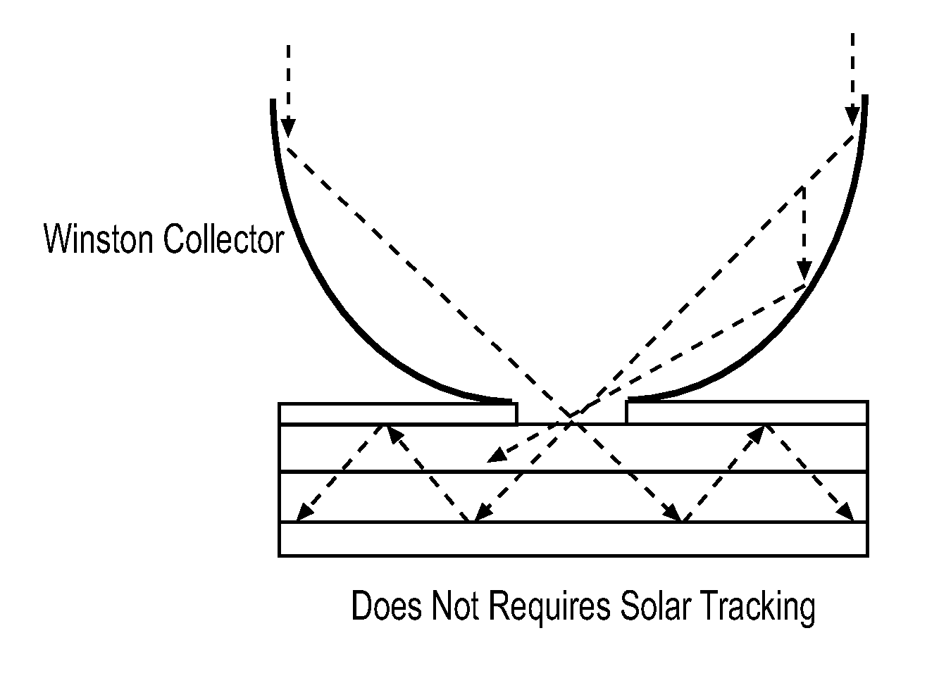
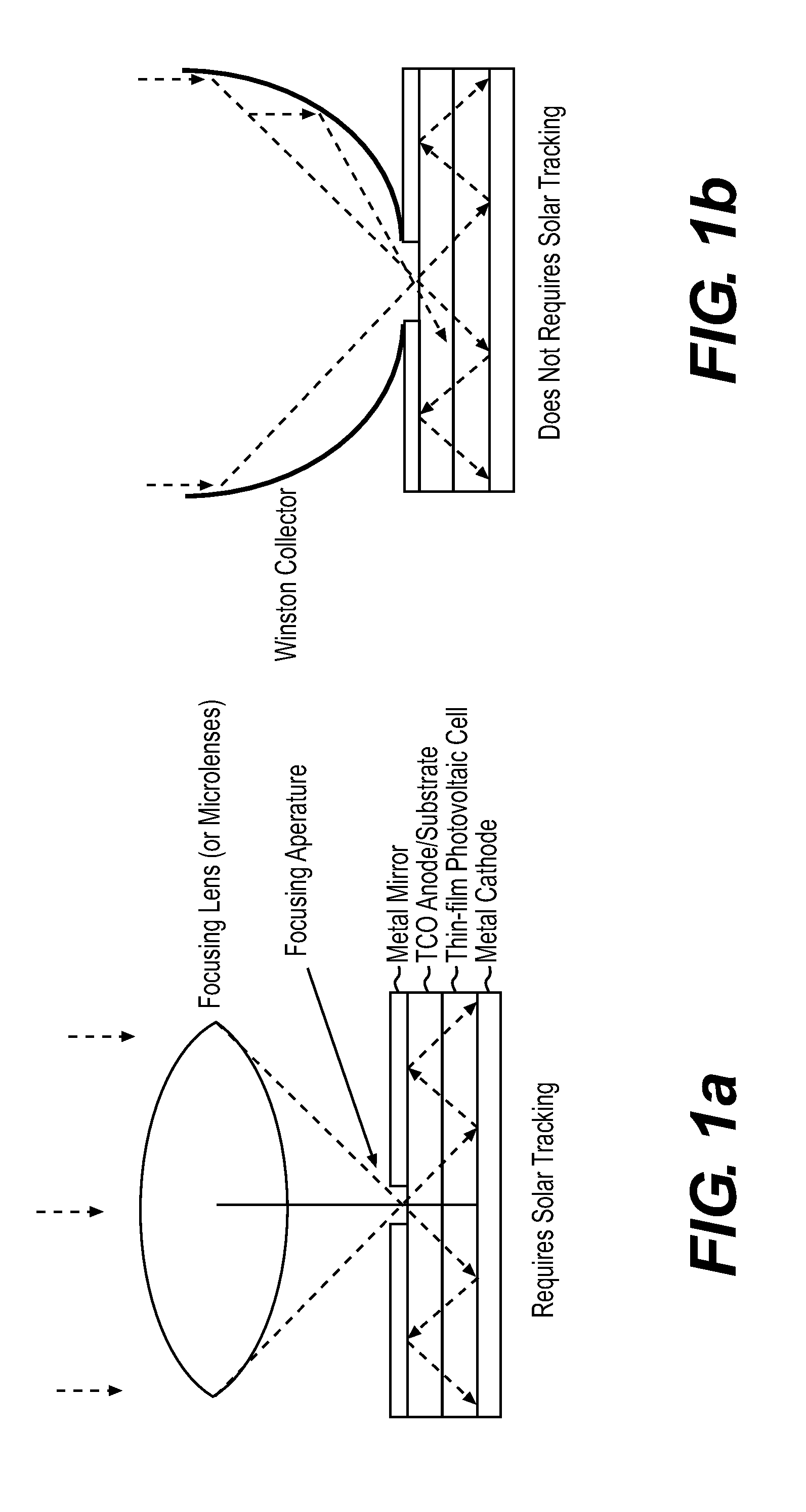
[0047]In FIG. 1, a cross-sectional view which can correspond to two different device structures is depicted. Both structures permit light to be introduced into a reflective cavity, or waveguide, containing photosensitive layers such that the light is initially incident in a direction generally perpendicular to the planes of the photosensitive layers. As a result, this type of structure is generally referred to herein as a “perpendicular type structure.”

[0048]Accordingly, light incident from the top of these embodiments enters into one or more concentrator structures (conical) or (trough-shaped). The light admitted to each concentrator is then reflected into an aperture or top reflective layer. The aperture is a generally circular shaped opening for use with a conical concentrator, and the aperture is a generally rectangular shaped opening for use with a trough-shaped concentrator. As the bottom surface layer is reflective, the top surface may be non-reflective and / or be optionally c...


PUM


Abstract

There is disclosed photovoltaic device structures which trap admitted light and recycle it through the contained photosensitive materials to maximize photoabsorption. For example, there is disclosed a photosensitive optoelectronic device comprising: a first reflective layer comprising a thermoplastic resin; a second reflective layer substantially parallel to the first reflective layer; a first transparent electrode layer on at least one of the first and second reflective layer; and a photosensitive region adjacent to the first electrode, wherein the first transparent electrode layer is substantially parallel to the first reflective layer and adjacent to the photosensitive region, and wherein the device has an exterior face transverse to the planes of the reflective layers where the exterior face has an aperture for admission of incident radiation to the interior of the device.

Description

CROSS-REFERENCE TO RELATED APPLICATION[0001]This application claims the benefit of U.S. Provisional Application No. 61 / 476,683, filed Apr. 18, 2011, which is incorporated herein by reference in its entirety.STATEMENT REGARDING FEDERALLY SPONSORED RESEARCH[0002]This invention was made with U.S. Government support under Contract No. FA9550-07-1-0364 awarded by the Air Force Office of Scientific Research and DE-FG36-08G018022 awarded by the Department of Energy. The government has certain rights in this invention.JOINT RESEARCH AGREEMENT[0003]The claimed invention was made by, on behalf of, and / or in connection with one or more of the following parties to a joint university-corporation research agreement: The University of Michigan and Global Photonic Energy Corporation. The agreement was in effect on and before the date the invention was made, and the claimed invention was made as a result of activities undertaken within the scope of the agreement.FIELD OF THE DISCLOSURE[0004]The pres...

Claims


Application Information

Patent Timeline
Patent Type & Authority Applications(United States)
IPC IPC(8): H01J40/04
CPCH01L31/0232H01L51/4246H01L51/447H01L31/0543Y02E10/52Y02E10/549H01L31/0547G02B5/0808H10K30/211H10K30/87H10K30/00
Inventor FORREST, STEPHEN R.LUNT, RICHARD R.SLOOTSKY, MICHAEL
Owner RGT UNIV OF MICHIGAN
Why Eureka
Try Eureka