Devices with Semiconductor Hyperbolic Metamaterials

a metamaterial and semiconductor technology, applied in the field of metals, can solve the problems of difficult to achieve thin metal deposition, metal layers have inherent loss, and must be deposited extremely thin, so as to improve the permeability and light collection, the effect of enhancing heat dissipation

Active Publication Date: 2016-09-22
UNITED STATES OF AMERICA
View PDF11 Cites 7 Cited by
  • Summary
  • Abstract
  • Description
  • Claims
  • Application Information

AI Technical Summary

Benefits of technology

[0044]According to another aspect of the invention, a transistor such as a HEMT is built on or in a semiconductor hyperbolic metamaterial for enhanced dissipation of heat.
[0045]According to another aspect of the invention, a phototransistor such as a HEMT is built on or in a semiconductor hyperbolic metamaterial for enhanced responsivity.
[0046]According to another aspect of the invention, a solar cell is built on or in a semiconductor hyperbolic metamaterial for enhanced light collection.

Problems solved by technology

However, there are some disadvantages to making hyperbolic metamaterials with metal layers.
In particular, metal layers have inherent loss and must be deposited extremely thin.
Thin metal deposition is difficult to achieve without surface roughening, which creates additional optical-loss.
Highly doped oxides can be used, but the doping levels required for producing a plasma frequency in the near-infrared creates material defects that also lead to high optical-loss.

Method used


Image

  • Devices with Semiconductor Hyperbolic Metamaterials
  • Devices with Semiconductor Hyperbolic Metamaterials
  • Devices with Semiconductor Hyperbolic Metamaterials

Examples


Embodiment Construction

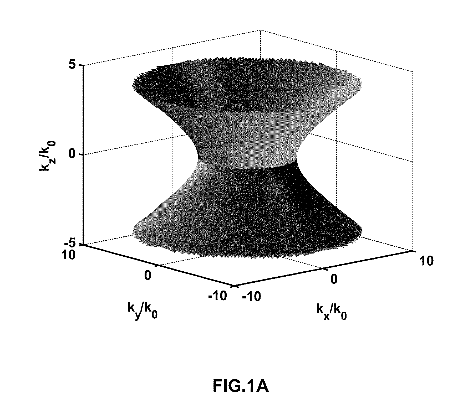
[0067]Light propagating in air with a certain angle relative to material slab (and thus kx wavevector) can only propagate into another material by matching the transverse wavevectors, e.g., kx-Air=kx-GaN. Light traveling from air at any angle relative to the GaN slab can propagate into the GaN given that a transverse component in GaN, kx-GaN, on the isofrequency curve is accessible for all possible transverse components in air, kx-Air. In contrast, only light propagating in GaN within a narrow angular cone relative to the air / GaN interface can propagate into the air by matching an available transverse wavevector in air. Light propagating in GaN at a larger angle relative to the surface normal cannot match the transverse wavevector and thus cannot propagate into the air, and will suffer from total internal reflection.

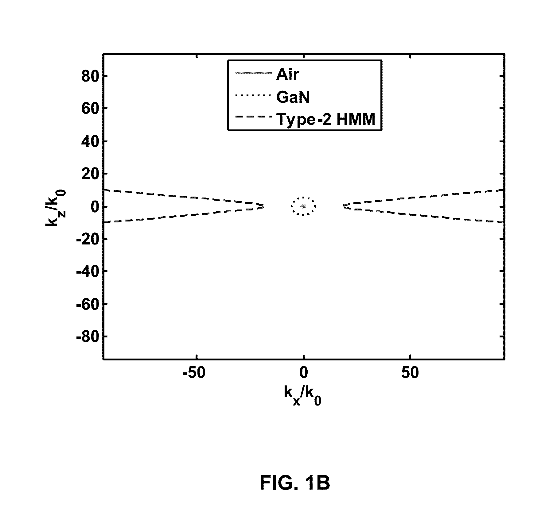
[0068]Examining FIG. 1B, one sees that any electromagnetic wave propagating in the type-2 hyperbolic metamaterial cannot match the transverse wavevector of air (or GaN) ...


PUM

PropertyMeasurementUnit
modulation frequencyaaaaaaaaaa
thicknessesaaaaaaaaaa
permittivityaaaaaaaaaa

Abstract

A hyperbolic metamaterial assembly comprising alternating one or more first layers and one or more second layers forming a hyperbolic metamaterial, the one or more first layers comprising an intrinsic or non-degenerate extrinsic semiconductor and the one or more second layers comprising a two-dimensional electron or hole gas, wherein one of in-plane or out-of-plane permittivity of the hyperbolic metamaterial assembly is negative and the other is positive.

Description

RELATED APPLICATIONS[0001]This application claims the benefit of U.S. Provisional Application No. 62 / 135,739, filed Mar. 20, 2015, which is hereby incorporated herein in its entirety.FIELD OF INVENTION[0002]The present invention relates generally to metamaterials, and more particularly to a devices with semiconductors hyperbolic metamaterials.BACKGROUND[0003]Permitivity, or ∈, describes electromagnetic (light) propagation in material. Metals have a permittivity less than zero while dielectrics have a permittivity greater than zero. In these “normal” materials, the permittivity is typically the same in all directions, thereby forming a sphere in k-space (momentum). However, hyperbolic metamaterials possesses components of opposite sign in the permittivity tensor,ɛ=[ɛxx000ɛyy000ɛzz],[0004]where the in-plane components themselves are equal ∈xx=∈yy but unequal to the perpendicular component ∈zz, that is, =∈yy. [C. L. Cortes, W. Newman, S. Molesky, Z. Jacob, Quantum nanophotonics using h...

Claims


Application Information

Patent Timeline
Patent Type & Authority Applications(United States)
IPC IPC(8): G02B6/122G02F1/017G02B6/42G02B6/126G02B6/12
CPCG02B6/1225G02B6/126G02B6/12004G02B2006/12123G02B6/4295G02F1/01708G02B6/4291G02F2202/30H01S5/1046H01S5/32341G02B1/002
Inventor MASTRO, MICHAEL A.
Owner UNITED STATES OF AMERICA
Why Eureka
Try Eureka