Solar Cell and Manufacturing Method Thereof

a technology of solar cells and manufacturing methods, applied in the field of solar cells, can solve the problems of deteriorating solar cell use efficiency and complicating processes of solar cells, and achieve the effects of improving solar cell efficiency, saving manufacturing time and cost, and simplifying the manufacturing process

Active Publication Date: 2012-11-01
SAMSUNG SDI CO LTD
View PDF11 Cites 27 Cited by
  • Summary
  • Abstract
  • Description
  • Claims
  • Application Information

AI Technical Summary

Benefits of technology

[0044]When the solar cell is manufactured using a silicon oxide used as a self-alignment mask according to embodiments of the present invention, the manufacturing process can be simplified and manufacturing time and cost can be saved. Further, since regions doped with opposite polarity are separated from each other, efficiency of the solar cell can be improved.

Problems solved by technology

The above-stated manufacturing method of the solar cell may complicate the processes due to increased number of processes for forming the doped regions and increased cost of manufacturing.
Thus, electron-hole pairs generated by photons from the contact areas can be easily recombined so that use efficiency of solar energy of the solar cell may be deteriorated.

Method used


Image

  • Solar Cell and Manufacturing Method Thereof
  • Solar Cell and Manufacturing Method Thereof
  • Solar Cell and Manufacturing Method Thereof

Examples


Embodiment Construction

[0054]A manufacturing method of a solar cell according to exemplary embodiments of the present invention will be described with reference to the accompanying drawings. Like reference numerals designate like parts and elements throughout the specification and the drawings. Further, various values are used in exemplary embodiments of the present invention, but the values do not limit the scope of the appended claims unless they are included within the spirit and scope of the appended claims.

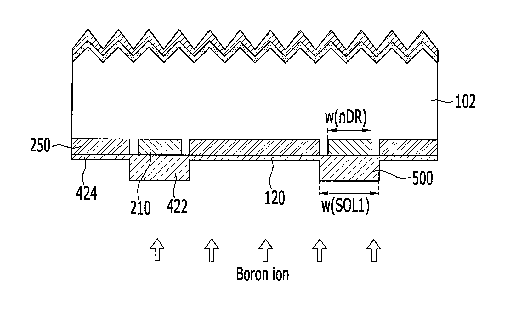
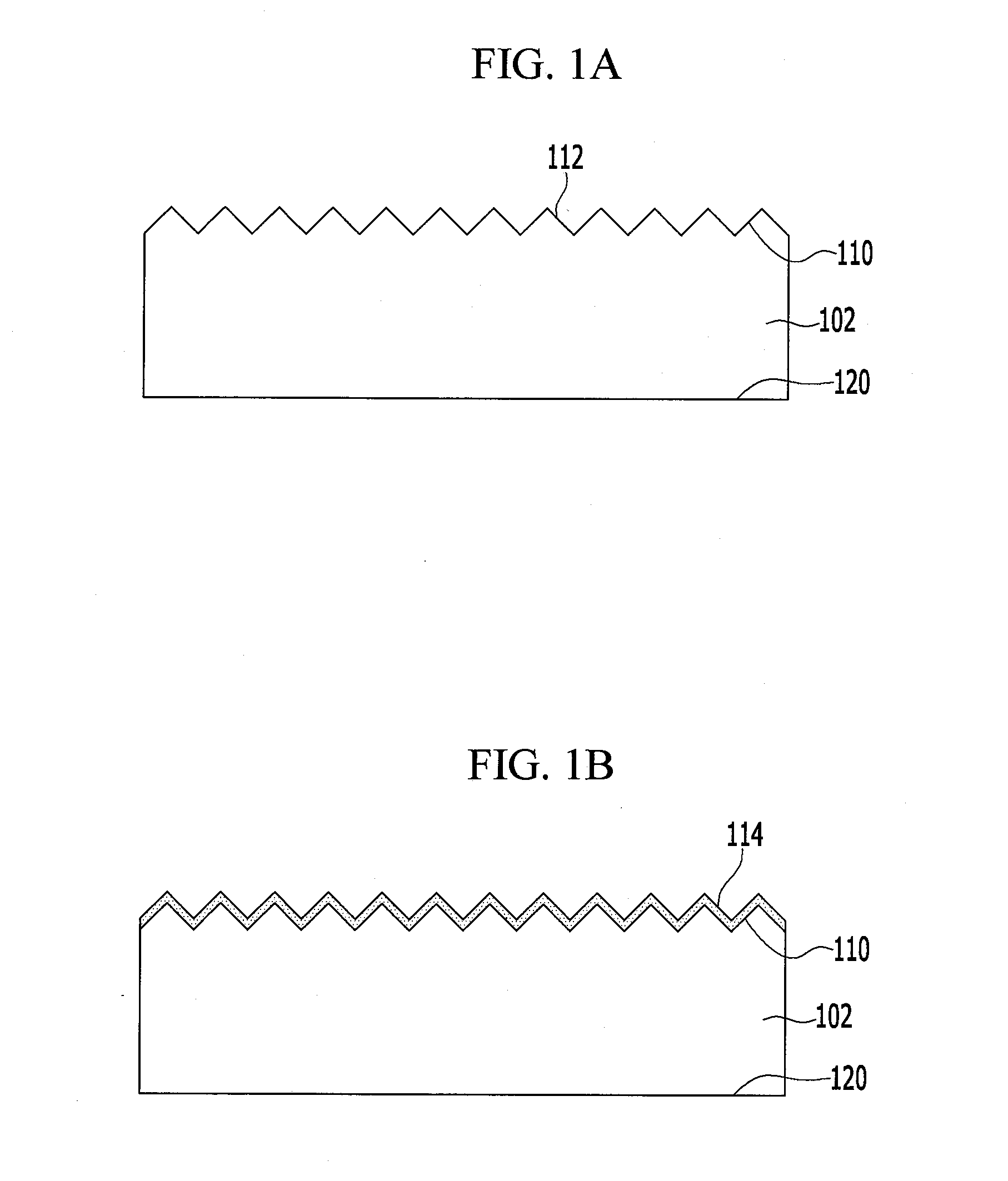
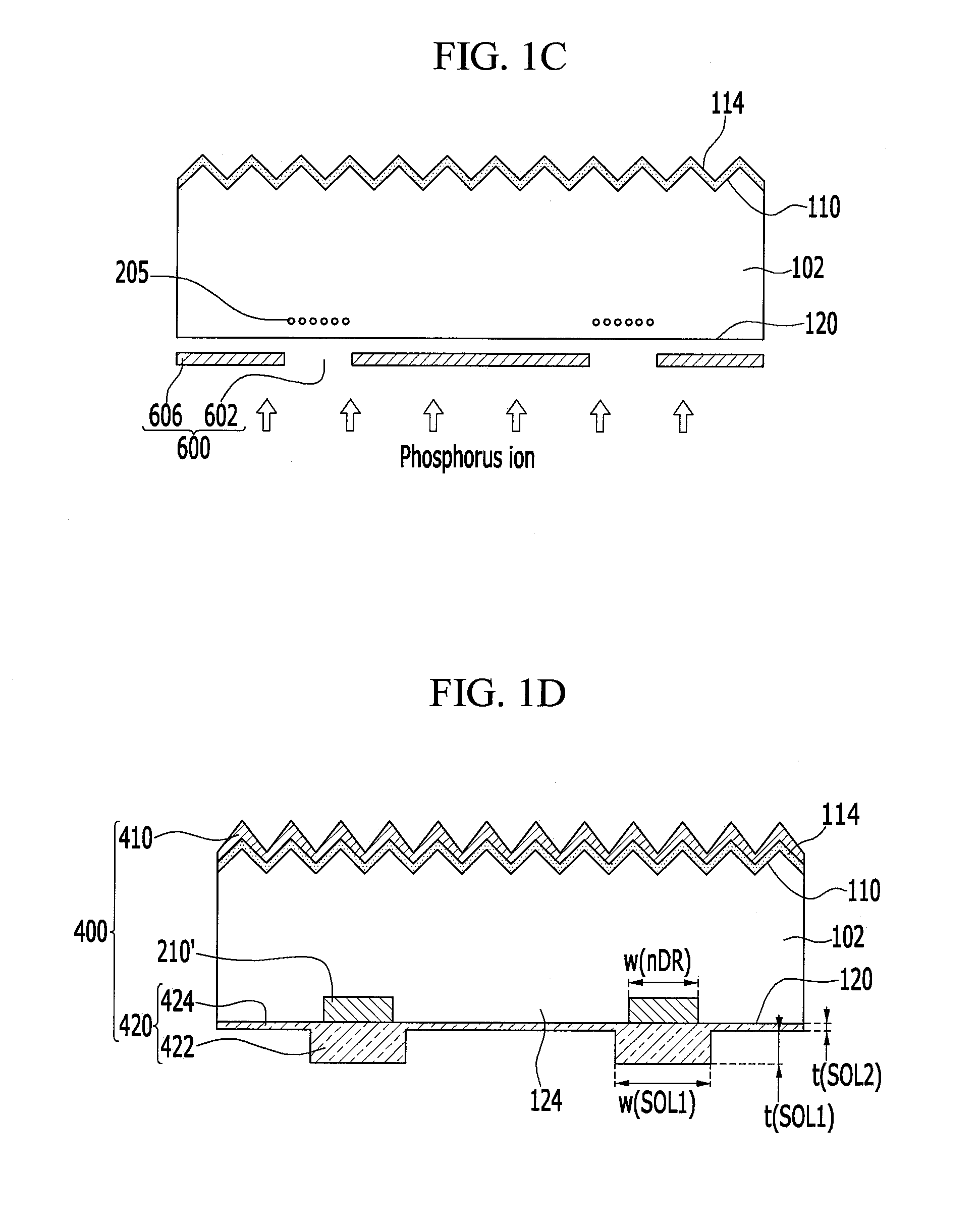
[0055]FIG. 1A to FIG. 1G are schematic cross-sectional views of processes for manufacturing a back contacting solar cell according to an exemplary embodiment of the present invention. Layers formed in front and back surfaces of a substrate are formed through the respective processes. According to an aspect of embodiments of the present invention, a silicon oxide layer grown on a surface of doped regions in the back surface of the substrate is thicker than a silicon oxide layer grown on an undoped r...


PUM


Abstract

A method for forming a doped region in a solar cell includes preparing a first and second surface of a substrate, forming a first doped region doped with a first dopant in a part of the first surface, forming a silicon oxide layer on the first surface, the silicon oxide layer including a first silicon oxide layer on the first doped region and having a first thickness, and a second silicon oxide layer on a portion of the first surface undoped by the first dopant and having a second thickness that is less than the first thickness, implanting a second dopant from outside the first surface into the first silicon oxide layer and the second silicon oxide layer, and forming a second doped region adjacent the first doped region by performing heat treatment on the first silicon oxide layer, the second silicon oxide layer, and the substrate.

Description

CROSS-REFERENCE TO RELATED APPLICATION[0001]This application claims priority to and the benefit of Korean Patent Application No. 10-2011-0041124 filed in the Korean Intellectual Property Office on Apr. 29, 2011, the entire content of which is incorporated herein by reference.BACKGROUND[0002]1. Field[0003]The described technology relates generally to a solar cell and a method manufacturing the same.[0004]2. Description of Related Art[0005]A solar cell includes a silicon substrate, a region of which has a surface that is p-doped, and a region of which has a surface that is n-doped. When solar light is incident on the solar cell, that is, when photons enter into the substrate, electron-hole pairs are formed in the substrate, the generated electrons move to the n-doped region, and the generated holes move to the p-doped region. Due to the movement of the electrons and the holes, a photovoltaic effect is generated, and a potential difference occurs between ends of the p-n junction. In ad...

Claims


Application Information

Patent Timeline
Patent Type & Authority Applications(United States)
IPC IPC(8): H01L31/0232H01L31/0236H01L31/18
CPCY02E10/547H01L31/0682
Inventor KIM, WON-GYUNKWAK, HEE-JUNEPARK, SANG-JINSEO, SANG-WONKIM, YOUNG-JIN
Owner SAMSUNG SDI CO LTD
Why Eureka
Try Eureka