Three-dimensional coherent plasmonic nanowire arrays for enhancement of optical processes

a plasmonic nanowire array and optical process technology, applied in the field of enhancement of optical processes, can solve the problems of reduced efficiency of collection aspect of any probing system, low uniformity and reproducibility on a large-area substrate, and process typically too weak to d

Inactive Publication Date: 2012-11-01
THE UNITED STATES OF AMERICA AS REPRESENTED BY THE SECRETARY OF THE NAVY
View PDF10 Cites 39 Cited by
  • Summary
  • Abstract
  • Description
  • Claims
  • Application Information

AI Technical Summary

Benefits of technology

[0009]The aforementioned problems are overcome in the present invention which provides a plasmonic grating sensor having vertically aligned periodic arrays of plasmonic nanopillars, nanowires, or both with an interparticle pitch from 200 to 2000 nm; a near-field coupled-plasmonic array sensor having vertically aligned periodic arrays of plasmonically coupled nanopillars, nanowires, or both with interparticle gaps small enough to induce overlapping evanescent plasmonic fields between neighboring particles (typically with edge-to-edge separations of <20 nm) within a large area, multiple particle architecture; and a plasmo-photonic array sensor having a double-resonance, periodic array of plasmonic nanoparticles distributed in subarrays of 1 to 25 plasmonically coupled nanopillars, nanowires, or other nanoparticles such as colloids where the subarrays are periodically spaced at a pitch on the order of a wavelength of light (λ / 8<pitch<3λ; λ=incident wavelength).

Problems solved by technology

However, for trace levels (ppm or lower) of chemical species these processes are typically too weak to detect without some method of enhancing the optical process (signal level).
This further adds to reduced efficiency in the collection aspect of any probing system.
While such approaches are ideal for near-field measurements such as NSOM or single molecule detection via SERS or SEFS, this also leads to very low uniformity and reproducibility on a large-area substrate.
These substrates are designed to maximize the SERS and / or SEFS intensity, but do not attempt to benefit from plasmonic coupling between closely-spaced nanostructures, long-range plasmonic coupling from large arrays of such nanostructures or from patterning these structures into a 1D or 2D diffraction gratings, whereby providing directionality and reduced divergence for the emitted and / or scattered irradiation.

Method used


Image

  • Three-dimensional coherent plasmonic nanowire arrays for enhancement of optical processes
  • Three-dimensional coherent plasmonic nanowire arrays for enhancement of optical processes
  • Three-dimensional coherent plasmonic nanowire arrays for enhancement of optical processes

Examples


Embodiment Construction

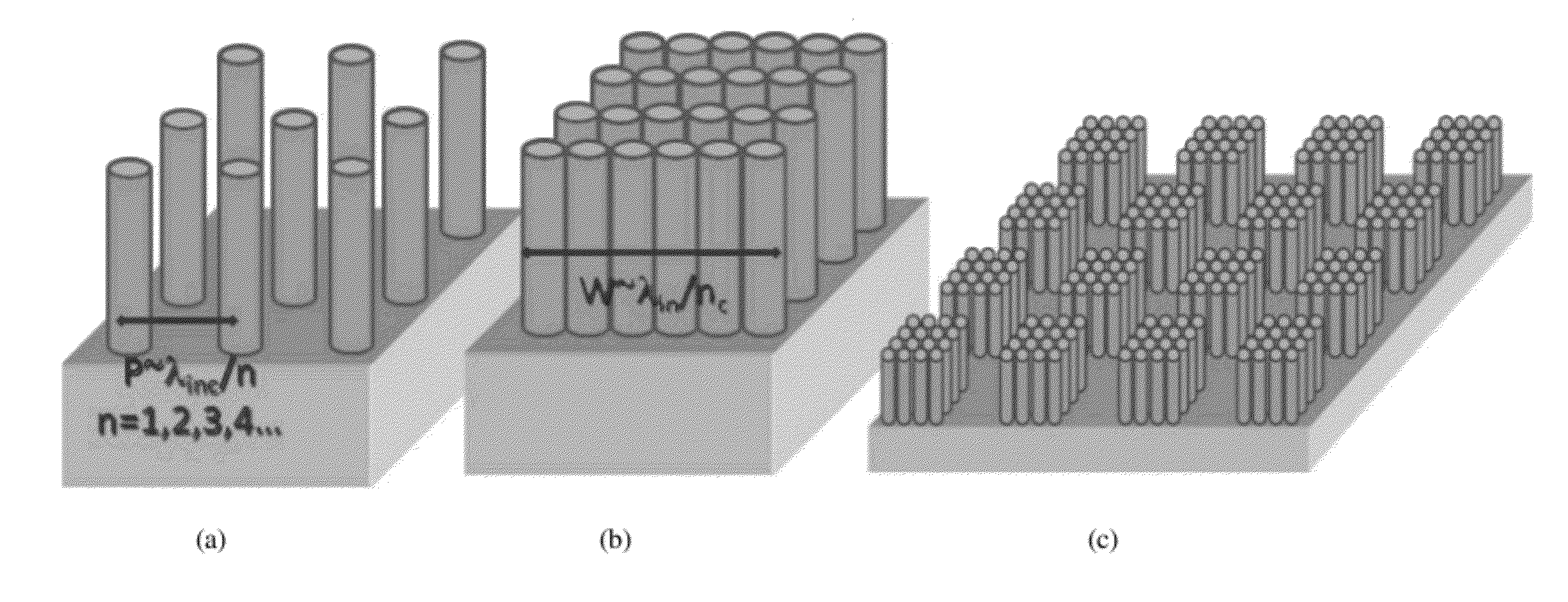
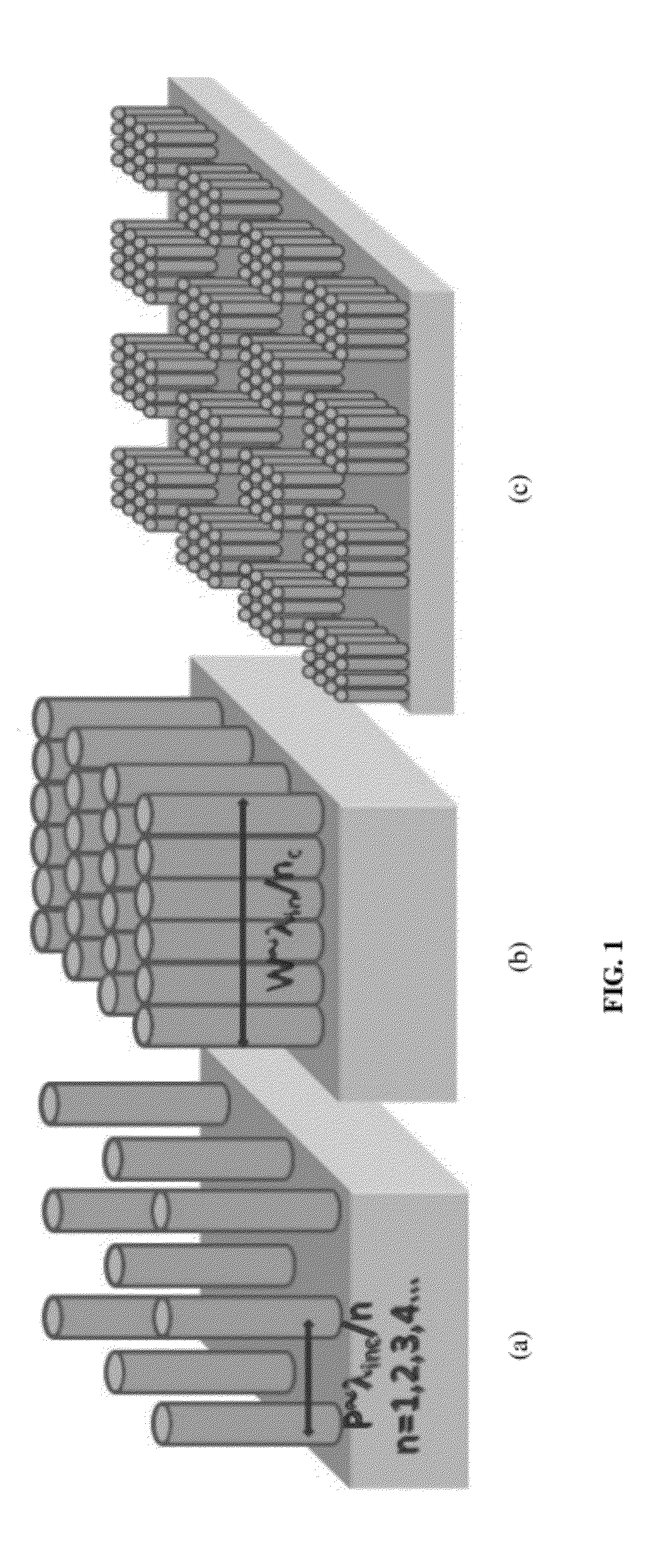
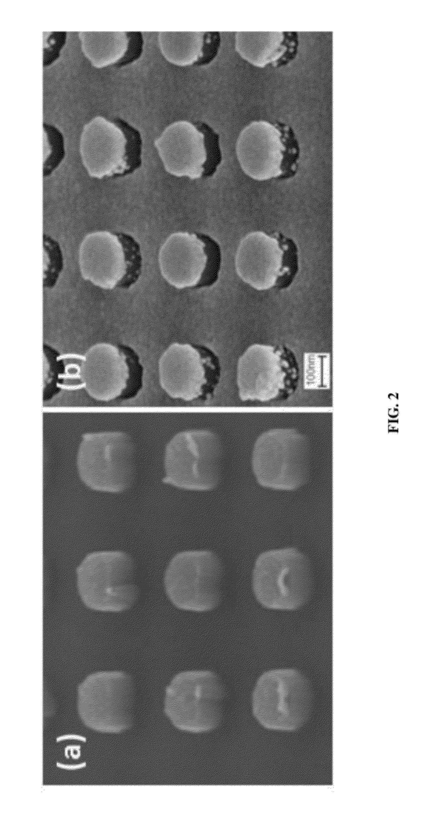
[0018]The present invention pertains to three arrayed plasmonic architectures that solve the need for a large area sensor with high signal uniformity and reproducibility, while maintaining high average SERS enhancement factors. The first structure is the plasmonic-grating sensor, which comprises periodic arrays of plasmonic nanoparticles with the interparticle pitch being on the order of a wavelength of light within the medium (λ / neff; neff is the effective index of refraction for the material chosen) in the UV-Vis-NIR region of the electromagnetic spectrum (200-2000 nm). The second structure is the coupled-plasmonic array sensor, which comprises periodic arrays of plasmonically coupled nanopillars / nanowires with interparticle gaps small enough to enable overlap between the evanescent fields from neighboring plasmonic nanoparticles, which typically requires edge-to-edge separations between the nanoparticles of less than 20 nm The third structure is the plasmo-photonic array sensor, ...


PUM


Abstract

A plasmonic grating sensor having periodic arrays of vertically aligned plasmonic nanopillars, nanowires, or both with an interparticle pitch ranging from λ/8−2λ, where λ is the incident wavelength of light divided by the effective index of refraction of the sample; a coupled-plasmonic array sensor having vertically aligned periodic arrays of plasmonically coupled nanopillars, nanowires, or both with interparticle gaps sufficient to induce overlap between the plasmonic evanescent fields from neighboring nanoparticles, typically requiring edge-to-edge separations of less than 20 nm; and a plasmo-photonic array sensor having a double-resonant, periodic array of vertically aligned subarrays of 1 to 25 plasmonically coupled nanopillars, nanowires, or both where the subarrays are periodically spaced at a pitch on the order of a wavelength of light.

Description

CROSS-REFERENCE TO RELATED APPLICATIONS[0001]This Application claims the benefit of U.S. Provisional Application 61 / 478,987 filed on Apr. 26, 2011 by Joshua D. Caldwell et al. entitled “THREE-DIMENSIONAL COHERENT PLASMONIC NANOWIRE ARRAYS FOR ENHANCEMENT OF OPTICAL PROCESSES,” the entire contents of which are incorporated herein by reference.BACKGROUND OF THE INVENTION[0002]1. Field of the Invention[0003]The present invention relates generally to enhancing optical processes and more specifically to plasmonic nanowire arrays for enhancement of optical processes.[0004]2. Description of the Prior Art[0005]Optical processes such as Raman scattering and fluorescence are very useful in identifying materials of interest from their optical or vibrational signatures. However, for trace levels (ppm or lower) of chemical species these processes are typically too weak to detect without some method of enhancing the optical process (signal level). In addition, the light scattered via the Raman pr...

Claims


Application Information

Patent Timeline
Patent Type & Authority Applications(United States)
IPC IPC(8): G01J1/42
CPCG01N21/658
Inventor CALDWELL, JOSHUA D.GLEMBOCKI, OREST J.PROKES, SHARKA M.RENDELL, RONALD W.
Owner THE UNITED STATES OF AMERICA AS REPRESENTED BY THE SECRETARY OF THE NAVY
Why Eureka
Try Eureka