Device for protecting an electric and/or electronic component arranged on a carrier substrate against electrostatic discharges

a technology for electric and/or electronic components, applied in the direction of coupling device connections, sustainable manufacturing/processing, final product manufacturing, etc., can solve the problems of increasing production costs, inability to prevent overvoltage, and complex mechanical and expensive design of the entire design

Inactive Publication Date: 2002-10-17
ROBERT BOSCH GMBH
View PDF4 Cites 44 Cited by
  • Summary
  • Abstract
  • Description
  • Claims
  • Application Information

AI Technical Summary

Benefits of technology

[0005] In principle, the electroconductive structures and the gap separating the conductive structures can be produced in widely differing manners. However, it is particularly advantageous to construct the electroconductive structures in the form of printed circuit traces which are configured on a shared main surface of the carrier substrate and which have mutually facing projections that are separated from each other by a gap produced in a defined manner. The printed circuit traces can be produced inexpensively on the main surface of the carrier substrate using known manufacturing methods. Because the mutually facing projections of the printed circuit traces taper in cross-section starting from the printed circuit traces, it is ensured that a defined sparkover takes place between the projection ends facing one another. In one advantageous exemplary embodiment, the projections taper essentially in the shape of a triangle and have pointed ends facing one another. The clearance between the pointed ends defines the gap width. Since here the spark discharge takes place directly on the surface of the carrier substrate, the disruptive discharge voltage in the gap is advantageously reduced by creeping spark discharges on the surface of the carrier substrate.
[0006] For example, the gap between the mutually facing projections of the conductive structures can be produced using etching techniques known from printed-circuit-board technology. It may be particularly advantageous if the gap between the mutually facing projections of the first and second electroconductive structures is produced by a laser cutting introduced into the printed-circuit-trace structures of the carrier substrate. Extremely small gaps can be made with great precision using the laser. In this way, it is possible to realize small gap widths to 20 micrometers, so that a sparkover takes place in the gap in the case of small disruptive discharge voltages. In addition, the formation time for the spark channel can thereby be minimized. Gap widths between 30 and 40 .mu.m may be preferable.
[0011] In another exemplary embodiment, the electroconductive structures are formed by two discrete conductor elements that project from the carrier substrate and are conductively connected to printed circuit traces of the carrier substrate. The ends of the conductor elements not connected to the carrier substrate face one another and are separated from one another by a defined gap. The spark discharge then comes about in the air gap between the ends of the conductor elements. It may be that this design approach is somewhat more complicated than the integration of the structures into the printed circuit traces of the carrier substrate. However, discrete conductor elements, such as metallic contact pins, exhibit great stability with respect to environmental influences, so that fluctuations in the gap width caused by environmental influences are negligibly small.
[0013] Another exemplary embodiment provides for the mutually facing sections, separated by the definably produced gap, of two printed circuit traces configured on the side of the carrier substrate fitted with components may be overlapped by an additional active or passive electrical component applied on the carrier substrate. The component covering the gap advantageously protects it from impurities and the deposit of conductive particles which could cause a short circuit between the two printed circuit traces. The active or passive component can be parallel-connected with respect to the discharge path, by electroconductively connecting a first terminal of the component to the first printed circuit trace jeopardized by a possibly occurring overvoltage, and electroconductivley connecting a second terminal of the component to the second printed circuit trace connected to the ground connection. Furthermore, to protect the discharge gap, the component may be joined in its edge area to the carrier substrate by an adhesive agent which seals the interspace between the component and the carrier substrate.

Problems solved by technology

Upon further insertion of the male connector, the contact spring element is separated from the contact elements, and the plug contacts are subsequently slid onto the contact elements; in so doing, it is not possible to prevent overvoltages present at an individual plug pin from being transferred to the contact elements of the carrier substrate, and from there to the components.
In addition, the entire design is relatively complicated mechanically and expensive.
In addition, production costs are thereby increased.
It may be that this design approach is somewhat more complicated than the integration of the structures into the printed circuit traces of the carrier substrate; however, discrete conductor elements, such as metallic contact pins, exhibit great stability with respect to environmental influences, so that fluctuations in the gap width caused by environmental influences are negligibly small.

Method used


Image

  • Device for protecting an electric and/or electronic component arranged on a carrier substrate against electrostatic discharges
  • Device for protecting an electric and/or electronic component arranged on a carrier substrate against electrostatic discharges
  • Device for protecting an electric and/or electronic component arranged on a carrier substrate against electrostatic discharges

Examples


Embodiment Construction

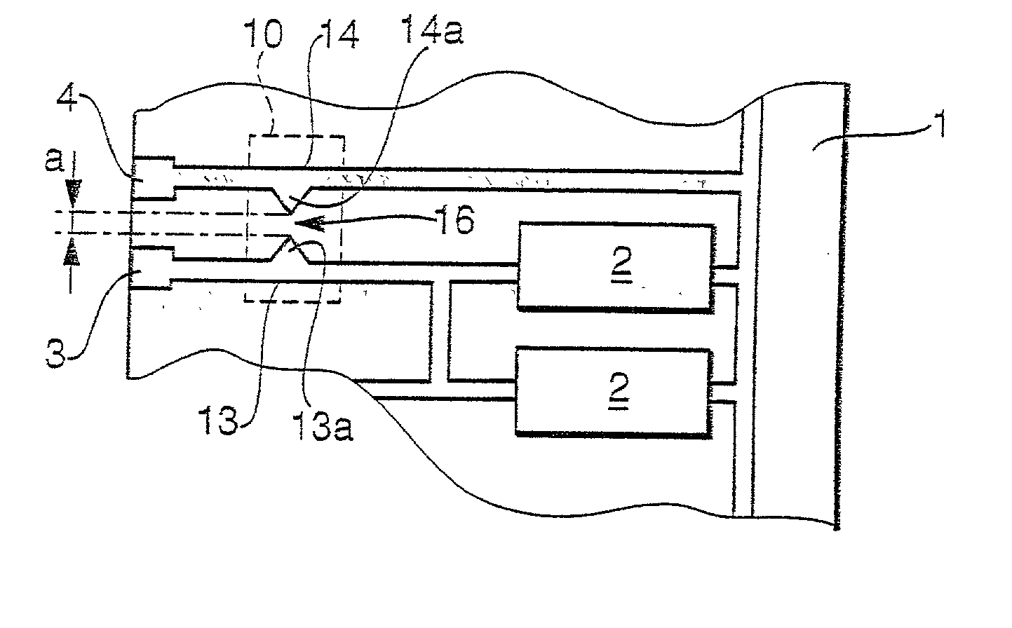
FIG. 1 shows a top view of the surface of a printed-circuit board 1, upon which a plurality of electrical and / or electronic components 2, e.g. microprocessors, storage components, semi-conductor chips, resistance components, inductive components or others are arranged. Printed-circuit board 1 is provided on one side with contact areas 3, 4 which are used for connecting the printed-circuit board to a male connector, contact area 3 being provided, for example, for the connection of a signal line, and contact area 4 being provided for the connection of a grounding contact to printed-circuit board 1. As FIG. 1 further shows, contact area 3 is connected via a printed circuit trace to the input of a component 2. Contact area 4 is connected via a further printed circuit trace 14 to the grounding contact of components 2. Grounding printed circuit trace 14 does not necessarily have to be connected to the grounding contact of components 2. Here, 415836 -8it can be any printed circuit trace wh...


PUM


Abstract

The proposal relates to a device for protecting an electrical and / or electronic component, arranged on a carrier substrate, from electrostatic discharges, an overvoltage occurring in the case of discharge at a carrier-substrate contact element connected to the component being diverted to a ground connection, bypassing the component. It is proposed that the protective device include a first electroconductive structure conductively connected to the jeopardized contact element, and a second electroconductive structure arranged adjacent to the first structure on the carrier substrate and conductively connected to the ground connection. Mutually facing sections of the electroconductive structures are set apart spatially from one another by a defined gap in such a way that an overvoltage transmitted to the contact element is transferred by a spark discharge in the gap from the section of the first electroconductive structure to the section of the second electroconductive structure, and is diverted to the ground connection.

Description

[0001] The present invention relates to a device for protecting an electrical and / or electronic component, arranged on a carrier substrate, from electrostatic discharges. Such devices are also known as ESD protective devices (ESD=electrostatic discharge).BACKGROUND INFORMATION[0002] In the course of inadvertent touching of contact elements of the carrier substrate, or when putting a male connector on the contact elements, or after installation of the carrier substrate in an electrical device, electrostatic discharges may be created. ESD protective devices on carrier substrates are used to prevent electrostatic discharges and ESD pulses from being transferred to the sensitive electronic components of the carrier substrate that are connected to the contact elements in the event that connectors, cable harness and aggregates receive voltage. The discharge current is diverted to a ground connection by the ESD protective device before it can reach the components. Such an ESD protective de...

Claims


Application Information

Patent Timeline
Patent Type & Authority Applications(United States)
IPC IPC(8): H01T4/08H01R13/707H05K1/02H05K3/30H05K3/34H05K9/00
CPCH01T4/08H05K1/026H05K1/0272H05K3/305H05K2201/10636H05K9/0066H05K2201/09772H05K2201/10295H05K3/3442Y02P70/50
Inventor FAUSER, EDWINROOZENBEEK, HERMANSCHILLING, WOLFGANGSEITEL, HANSWIZEMANN, THOMASPFENDTNER, REINHARDBUTSCHKAU, WERNERHILLER, WOLFGANGJOSTEN, STEFAN
Owner ROBERT BOSCH GMBH
Why Eureka
Try Eureka