Plasma procesor and plasma processing method

a plasma processing and plasma technology, applied in the direction of chemical vapor deposition coating, electric discharge tubes, coatings, etc., can solve the problems of large portions of silicon oxide film of semiconductor wafers, abnormal discharge between, and most devices of semiconductor wafers becoming defective, so as to prevent undesired discharge and improve productivity.

Inactive Publication Date: 2011-11-15
TOKYO ELECTRON LTD
View PDF12 Cites 44 Cited by
  • Summary
  • Abstract
  • Description
  • Claims
  • Application Information

AI Technical Summary

Benefits of technology

[0023]It is, therefore, an object of the present invention to provide a plasma processing apparatus and a plasma processing method, which are ca...

Problems solved by technology

However, in the above conventional etching apparatuses, a plasma induces a considerable electric potential difference between electric potentials of the semiconductor wafer W and the focus ring 152 during an etching process, and the electric potential difference leads to a so-called surface arcing that causes an abnormal discharge between a surface of the semiconductor wafer W and the focus ring 152.
If the abnormal discharge occurs, large portions of the silicon oxide film of the semiconductor wafer are destroyed and most devices of the semiconductor wafer become defective.
Further, the inside of the etching chamber is contaminated with metal contaminants, which in turn makes it impossible to continue the etching process without cleaning the etching chamber, thereby significantly deteriorating overall productivity.
However, the arcing may be caused by some other factors, e.g., in a case where a semiconductor wafer is ecc...

Method used


Image

  • Plasma procesor and plasma processing method
  • Plasma procesor and plasma processing method
  • Plasma procesor and plasma processing method

Examples


Embodiment Construction

[0070]Hereinafter, preferred embodiments of the present invention will be described in detail with reference to the accompanying drawings.

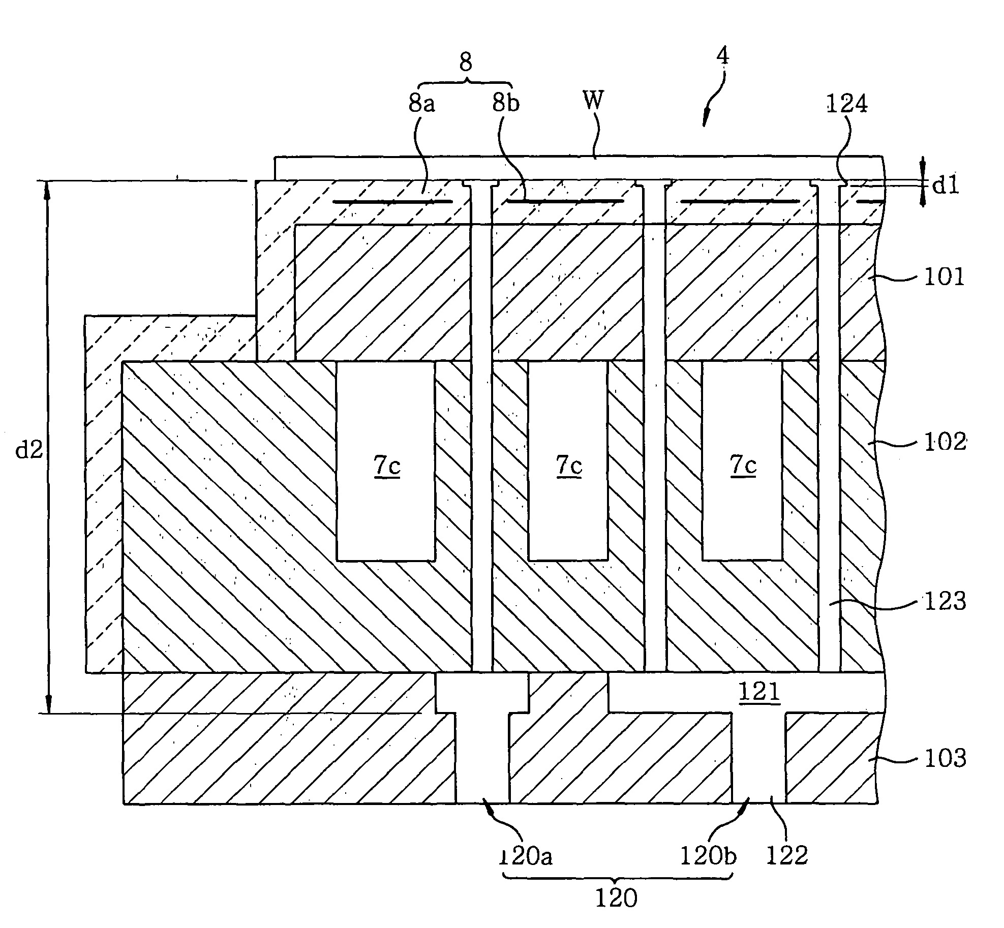
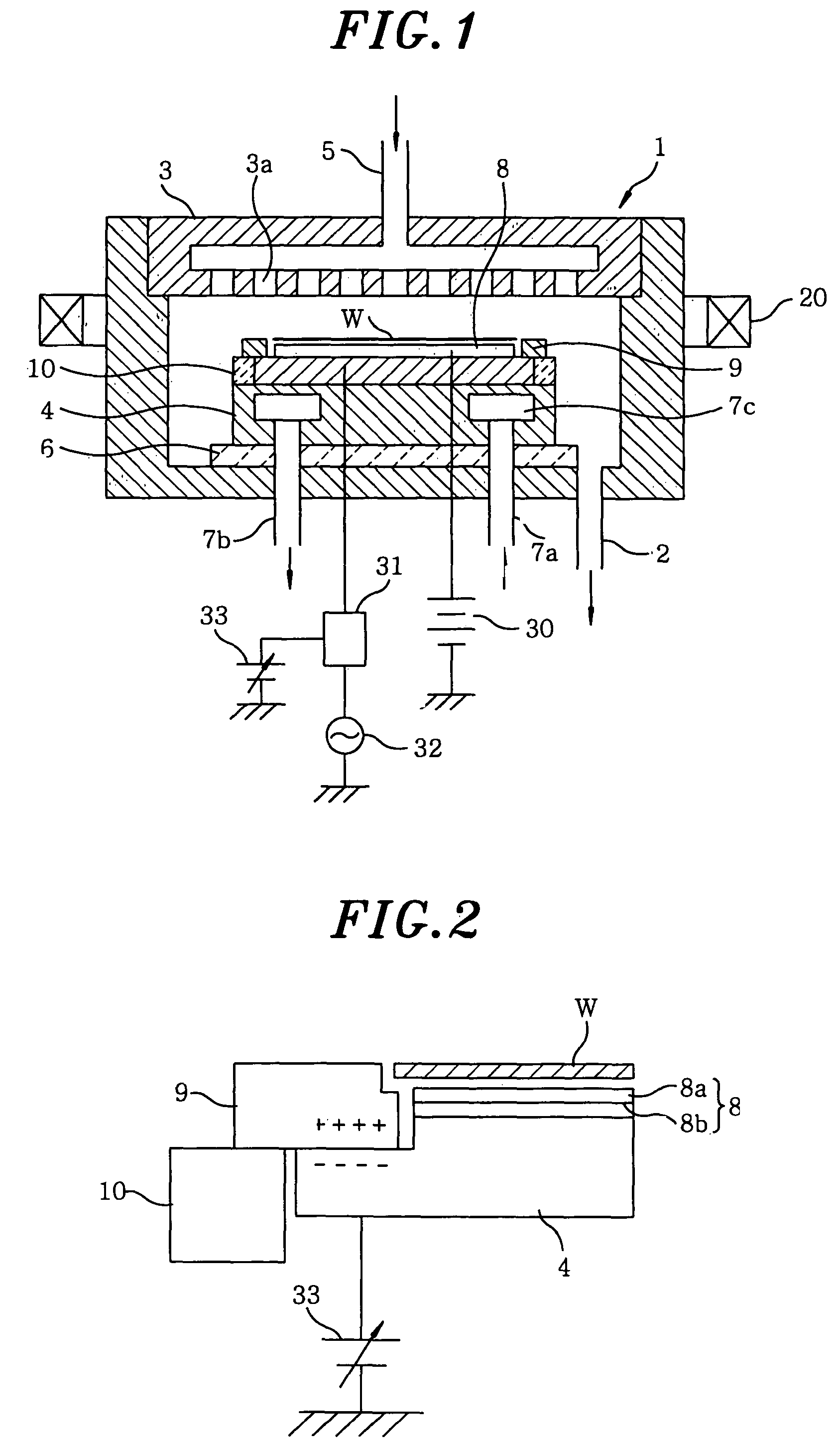
[0071]FIG. 1 schematically illustrates an overall configuration of a dipole magnetron plasma etching apparatus in accordance with a first preferred embodiment of the present invention. Reference numeral 1 indicates an etching chamber (a processing chamber). The etching chamber 1 is made of aluminum or the like of a cylindrical shape, and an inner portion thereof can be air-tightly sealed. Installed in a bottom portion of the etching chamber 1 is an exhaust line 2 connected to a vacuum pump (not shown) that is not illustrated, so that an inner space of the etching chamber 1 can be exhausted to a predetermined level of vacuum state.

[0072]Further, installed at a top portion and at the bottom portion of the etching chamber 1 are an upper electrode 3 facing downward and a lower electrode 4 facing the upper electrode 3, respectively.

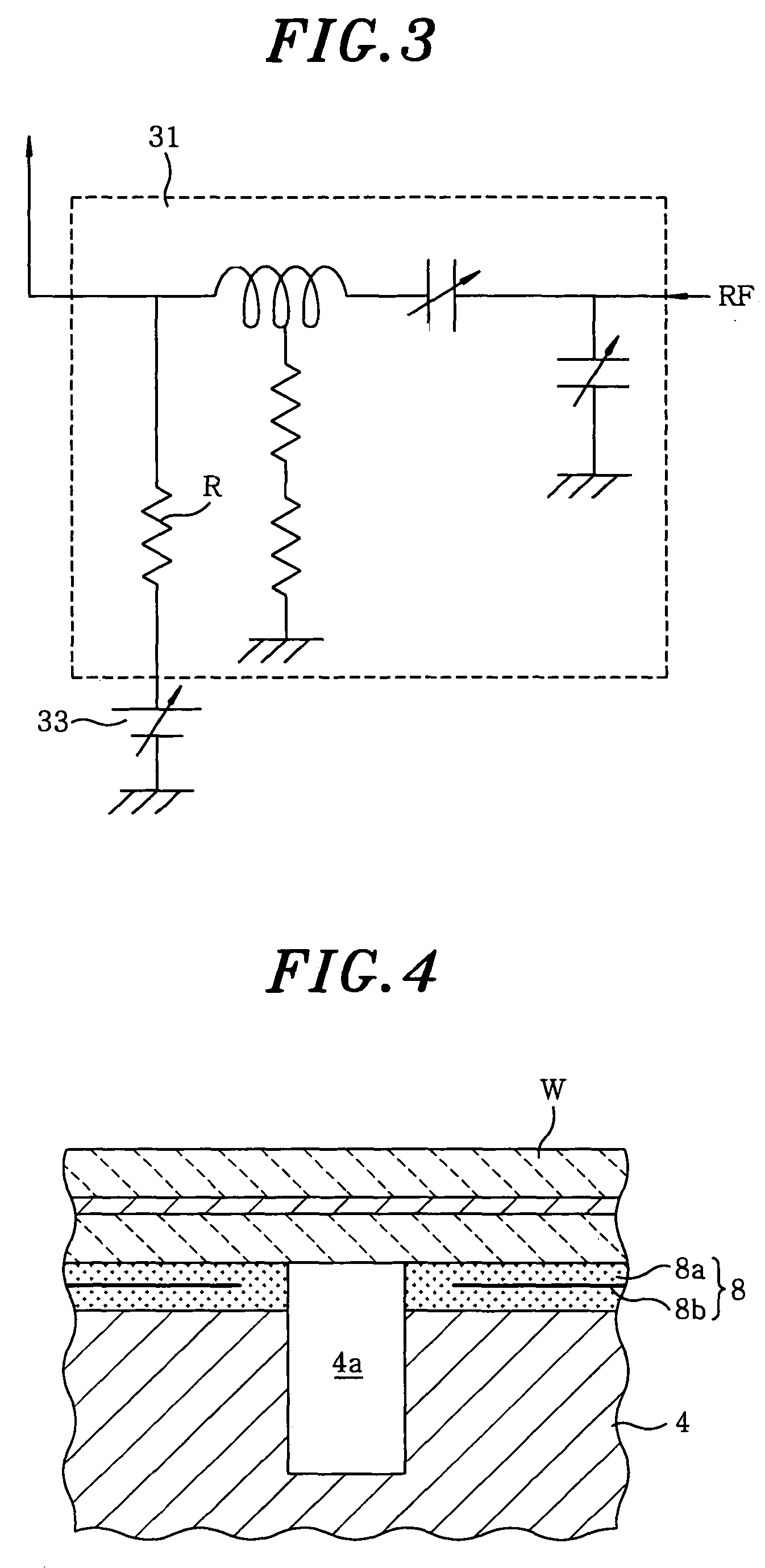
[0073]The upper elec...


PUM

PropertyMeasurementUnit
Depthaaaaaaaaaa
Distanceaaaaaaaaaa
Dimensionaaaaaaaaaa

Abstract

An etching chamber 1 incorporates a focus ring 9 so as to surround a semiconductor wafer W provided on a lower electrode 4. The plasma processor is provided with an electric potential control DC power supply 33 to control the electric potential of this focus ring 9, and so constituted that the lower electrode 4 is supplied with a DC voltage of, e.g., −400 to −600 V to control the electric potential of the focus ring 9. This constitution prevents surface arcing from developing along the surface of a substrate to be processed.

Description

FIELD OF THE INVENTION[0001]The present invention relates to a plasma processing apparatus and a plasma processing method for processing a substrate to be processed, e.g., a semiconductor wafer, by using a plasma.BACKGROUND OF THE INVENTION[0002]A plasma processing apparatus and a plasma processing method have been widely used for processing a substrate, e.g., a semiconductor wafer, by using a plasma. For example, an etching apparatus is commonly used in a semiconductor device manufacturing process as a technique for forming fine electric circuits on the semiconductor wafer by etching and removing a thin film formed on a semiconductor wafer by using a plasma.[0003]Such an etching apparatus includes a processing chamber (an etching chamber) whose inner space can be air-tightly sealed such that a plasma is generated in the etching chamber. A semiconductor wafer is mounted on a susceptor installed in the etching chamber and then etched.[0004]Among many known various types of apparatuse...

Claims


Application Information

Patent Timeline
IPC IPC(8): C23C16/50C23C16/52C23F1/00H01L21/306C23C16/06C23C16/22H01J37/32
CPCH01J37/32174H01J37/32642H01J37/3411H01L21/67069H01J37/3244H01J37/32532H01J37/32724H01J37/32715H01J2237/0206H01J2237/334H01J2237/002C23C16/45565C23C16/509C23C16/5096H01J37/32082H01J37/32623
Inventor KIKUCHI, AKIHIROKAYAMORI, SATOSHISHIMA, SHINYASAKAMOTO, YUICHIROHIGUCHI, KIMIHIROOOHASHI, KAORUUEDA, TAKEHIROSHIBUYA, MUNEHIROGONDAI, TADASHI
Owner TOKYO ELECTRON LTD
Why Eureka
Try Eureka