

Organic light emitting diode and method of manufacturing the same
a light-emitting diode and organic technology, applied in the direction of thermoelectric device junction materials, semiconductor devices, electrical apparatus, etc., can solve the problems of inability to form a stack, formation of organic light-emitting diode elements, and imbalance between the number of generated holes and the number of generated electrons, so as to improve stability
Inactive Publication Date: 2012-11-15
SAMSUNG ELECTRO MECHANICS CO LTD
View PDF2 Cites 8 Cited by
- Summary
- Abstract
- Description
- Claims
- Application Information
AI Technical Summary
Benefits of technology
[0015]An aspect of the present invention provides an organic light emitting diode and a method of manufacturing the same allowing for improved stability.
Problems solved by technology
However, existing lower layers may be removed during the formation of a new layer, such that it may be difficult to form a stack.
In addition, there are common problems in the formation of organic light emitting diode elements.
First, within a polymer organic thin film layer, holes have a moving speed faster than that of electrons, such that imbalance between the number of generated holes and the number of generated electrons may occur.
Second, oxygen or moisture may easily penetrate the organic layers to thereby permeate into the element, thereby deteriorating the performance and the stability of the element.
In addition, in the case of poly(3,4-ethylenedioxythiophene): poly(styrene sulfonate), widely used as a material of the hole injection layer, protrusion due to aging may be frequently generated, such that a short-circuit between electrodes occurs.
Method used
View moreImage
Smart ImageViewing Examples

Examples
first embodiment
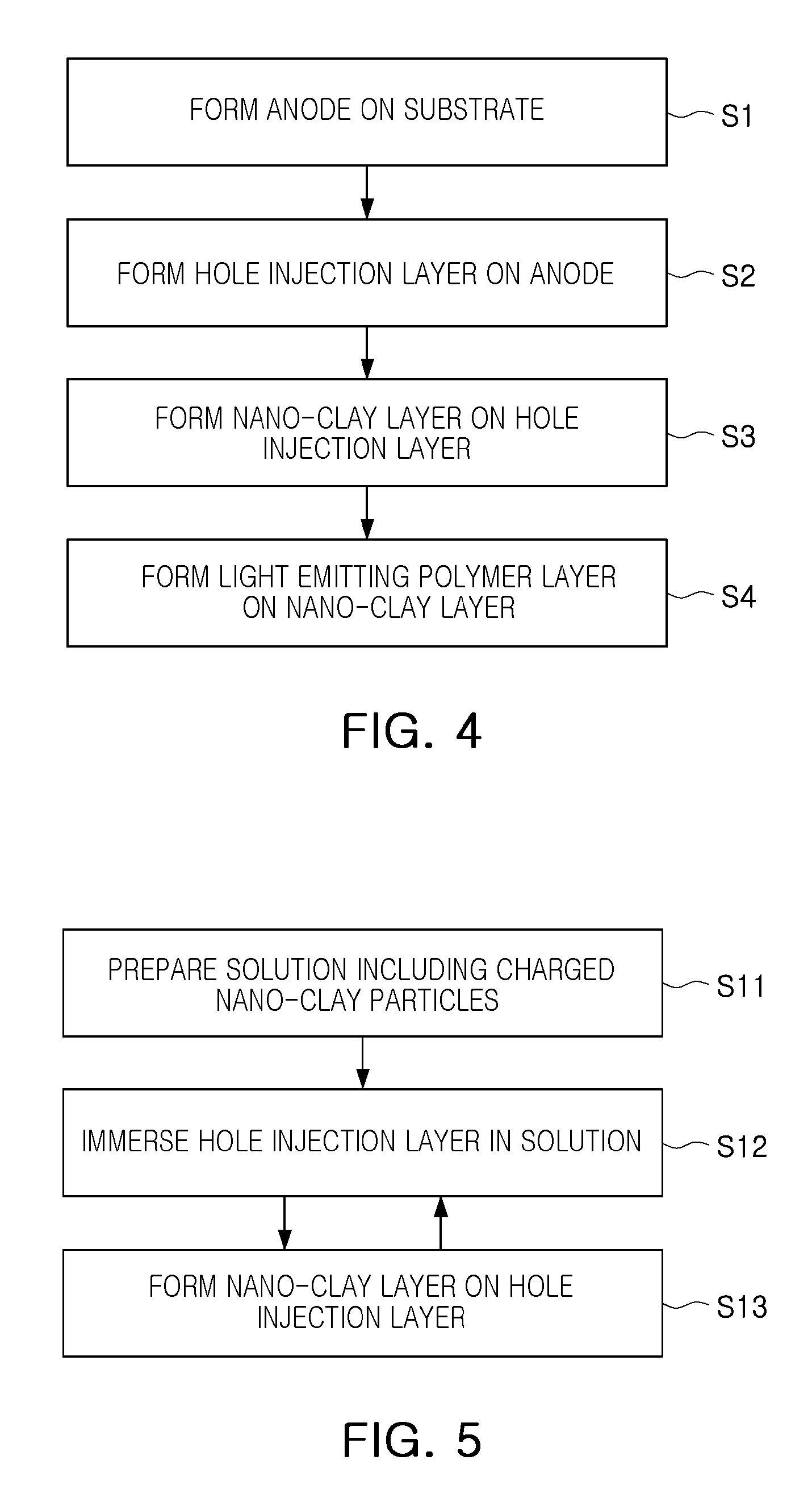
[0096]FIG. 5 is a flowchart showing a process of manufacturing a nano-clay layer of an organic light emitting diode according to the present invention.
second embodiment
[0097]FIG. 6 is a flowchart showing a process of manufacturing a nano-clay layer of an organic light emitting diode according to the present invention.
third embodiment
[0098]FIG. 7 is a flowchart showing a process of manufacturing a nano-clay layer of an organic light emitting diode according to the present invention.
Login to View More PUM
| Property | Measurement | Unit |
|---|---|---|
| thickness | aaaaa | aaaaa |
| thickness | aaaaa | aaaaa |
| surface area | aaaaa | aaaaa |
Abstract
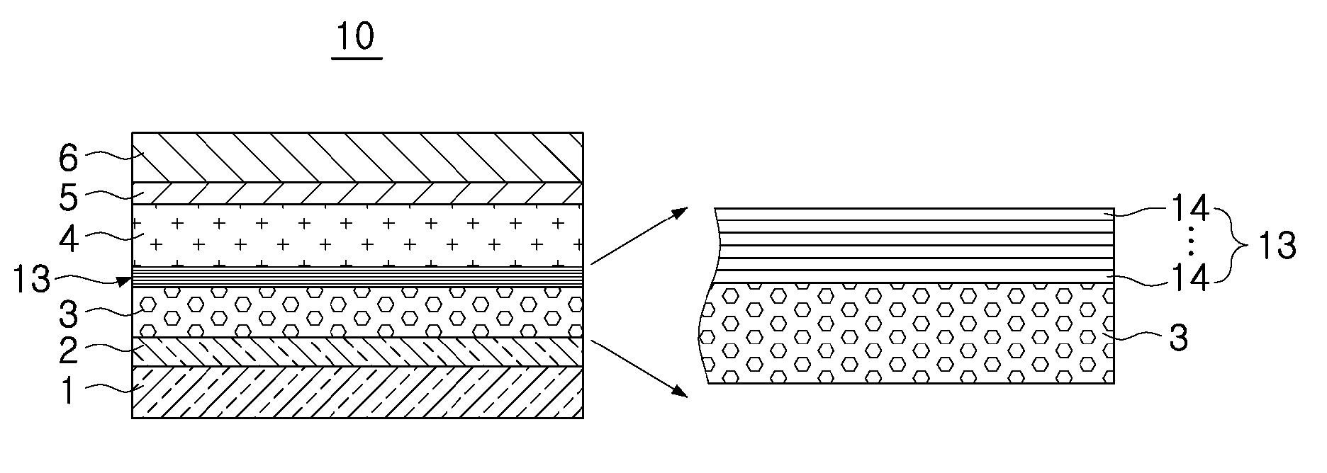
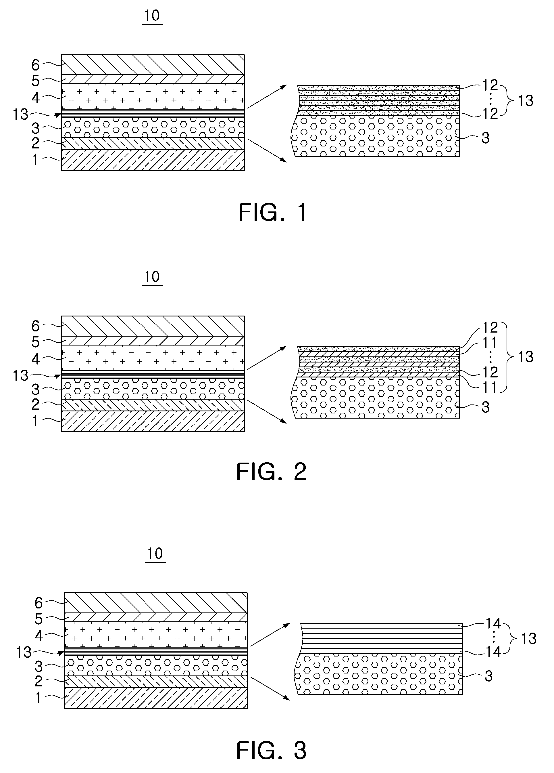
There are provided an organic light emitting diode and a method of manufacturing the same. The organic light emitting diode includes: an anode formed on a substrate; a protective layer having at least one inorganic material layer stacked therein, the at least one inorganic material layer containing at least one of a nano-clay and a graphite oxide; a light emitting polymer layer formed on the protective layer; and a cathode formed on the light emitting polymer layer. In the case of the organic light emitting diode, the injection concentration of holes may be controlled, such that the stability of an element may be improved and the lifespan thereof may be increased.
Description
CROSS-REFERENCE TO RELATED APPLICATIONS[0001]This application claims the priority of Korean Patent Application No. 10-2011-0044393 filed on May 12, 2011, in the Korean Intellectual Property Office, the disclosure of which is incorporated herein by reference.BACKGROUND OF THE INVENTION[0002]1. Field of the Invention[0003]The present invention relates to an organic light emitting diode and a method of manufacturing the same allowing for improved stability.[0004]2. Description of the Related Art[0005]An organic light emitting diode (OLED) recently used in the field of displays is a self-luminous display element and has a wide viewing angle, excellent contrast, and a fast response time.[0006]In addition, the organic light emitting diode is excellent in terms of brightness, driving voltage, and response speed characteristics, as compared to an inorganic electro-luminescence (EL) element, and may be polychromed, such that it has been prominent as a display element.[0007]A general organic ...
Claims
Login to View More Application Information
Patent Timeline
 Patent Type & AuthorityApplications(United States)
IPC IPC(8): H01L51/54H01L51/56H10N10/856
CPCH01L51/5253H01L51/5215H10K50/844H10K50/8445H10K85/10H10K2102/331H10K50/816
InventorLEE, KWANG JIKHAM, SUK JINLIM, JI HYUK
OwnerSAMSUNG ELECTRO MECHANICS CO LTD