Plasmonic In-Cell Polarizer

a plasmonic polarizer and in-cell technology, applied in the field of flat panel displays, can solve the problems of low optical efficiency, limited display integration capability, scattering of light, etc., and achieve the effects of reducing power consumption, improving visual performance, and high polarization performan

Inactive Publication Date: 2012-11-15
SHARP KK
View PDF11 Cites 19 Cited by
  • Summary
  • Abstract
  • Description
  • Claims
  • Application Information

AI Technical Summary

Benefits of technology

[0026]Described herein is an in-cell polarizer that can achieve high polarization performance at all the visible wavelengths including blue wavelength range (400-500 nm). Moreover, the polarizer can be easily integrated into a liquid crystal cell structure to realize a new type of LCD display with a better visual performance and lower power consumption, as compared to conventional LCD systems. For example, a polarizer operating in blue wavelength range would be useful for an LCD display with blue light emitting diode (LED) backlight that has color generating pixels that include red and green fluorescent layers, and a blue transmission layer.

Problems solved by technology

With no applied voltage, the liquid crystals are randomly arranged in the droplets, resulting in scattering of light as it passes through the window assembly.
However, some of the drawbacks to the conventional film polarizer are as follow: (1) a low optical efficiency with transmission values of 25˜30% for unpolarized light and 50˜60% for polarized light in the visible wavelength regime, with a typical extinction ratio value (Tper / Tpar) of ˜6000, (2) sensitivity to heat and humidity due to a film resin made from organic materials, and (3) limited display integration capability due to the need for a protective film such as tri-acetyl cellulose (TAC) film on both sides of polarizing layer.
However, some of the drawbacks of glass polarizer are as follow: (1) a high extinction ratio is only achievable in long visible to IR wavelength due to proprietary glass manufacturing processes, and (2) a low integration capability into devices such as in LCD pixel cell due to large thickness of glass substrate.
With this configuration, an unnecessary gap spacing is created between LC cell and phosphor layers, which causes optical cross-talk within the system, and therefore creates low contrast and poor visual performances in the display.
Also, the manufacturing costs would be significantly high due to the complex 3-glass substrate structure.

Method used


Image

  • Plasmonic In-Cell Polarizer
  • Plasmonic In-Cell Polarizer
  • Plasmonic In-Cell Polarizer

Examples


Embodiment Construction

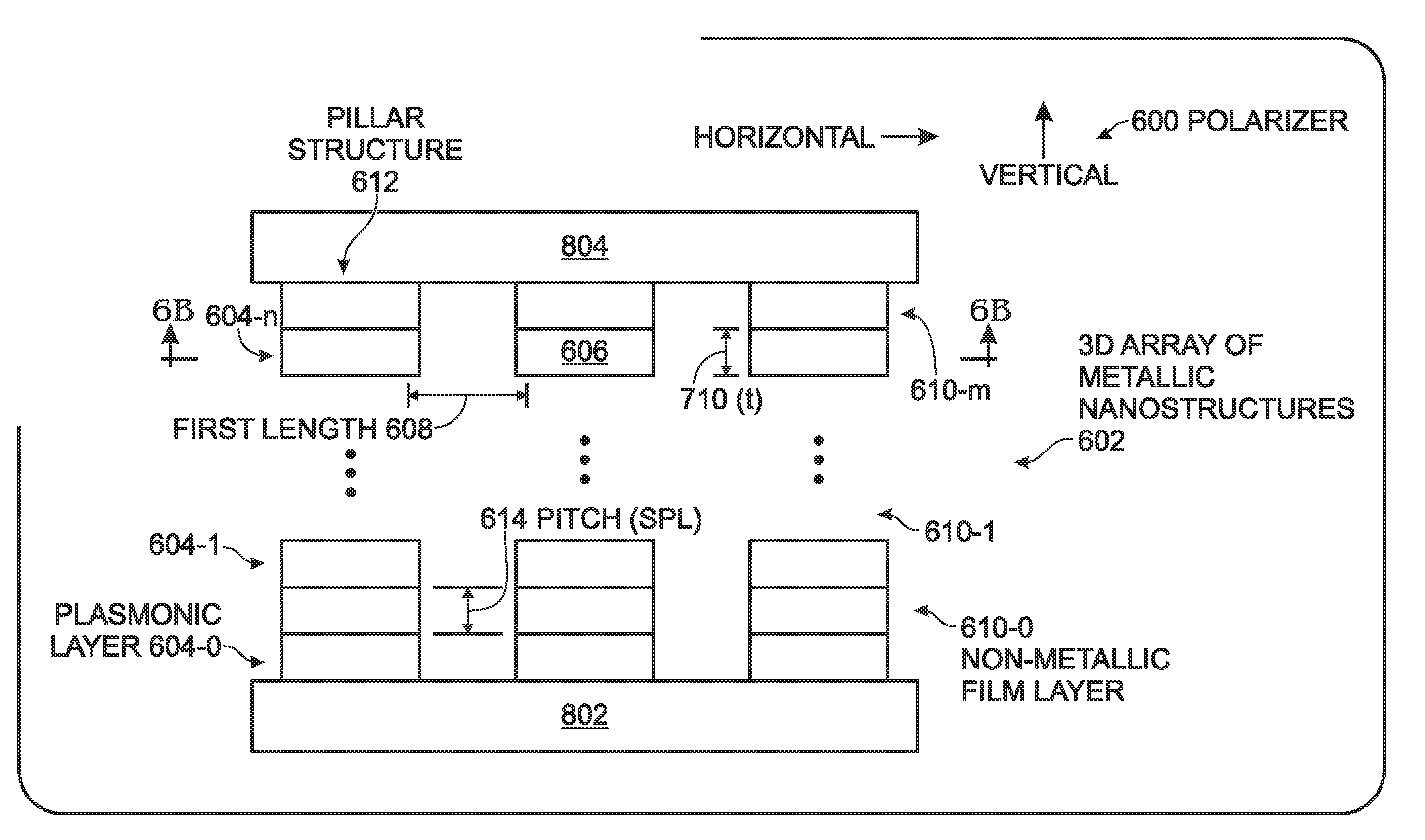
[0050]FIGS. 6A and 6B are, respectively, partial cross-sectional and plan views of a plasmonic polarizer. The polarizer 600 comprises a three-dimensional (3D) array of metallic nanostructures 602 comprising a plurality of plasmonic layers 604-0 through 604-n, where each layer includes a pattern of metallic nanostructures 606. The nanostructures 606 have dimensions and periods between adjacent nanostructures less than a first length 608, where the first length is equal to (a first wavelength of light / 2). For example, the first wavelength of light may be 450 nm. The 3D array of metallic nanostructures 602 also comprises a plurality of non-metallic film layers 610-0 through 610-m, with at least one non-metallic film layer interposed between adjacent plasmonic layers. The values of (n) and (m) are positive integer variables not limited to any particular value. The value of (m) need not necessarily equal the value of (n). Each non-metallic film layer may be comprised of a material transp...


PUM

PropertyMeasurementUnit
wavelengthaaaaaaaaaa
humidityaaaaaaaaaa
humidityaaaaaaaaaa

Abstract

A plasmonic polarizer and a method for fabricating the plasmonic polarizer are provided. The method deposits alternating layers of non-metallic film and metal, forming a stack. A hard mask is formed overlying the stack. The hard mask comprises structures having dimensions and periods between adjacent structures less than a first length, where the first length is equal to (a first wavelength of light/2). The stack is etched through openings in the hard mask to form pillar stacks of alternating non-metallic and metal layers having the dimensions of the hard mask structures. Then, the hard mask structures are removed. In one aspect, subsequent to removing the hard mask structures, the spaces between the pillar stacks are filled with a dielectric material.

Description

RELATED APPLICATION[0001]The application is a Continuation-in-Part of a pending application entitled, PLASMONIC REFLECTIVE DISPLAY FABRICATED USING ANODIZED ALUMINUM OXIDE, invented by Aki Hashimura et al., Ser. No. 13 / 449,370, filed on Apr. 19, 2012, Attorney Docket No. SLA3106;[0002]which is a Continuation-in-Part of a pending application entitled, METHOD FOR IMPROVING METALLIC NANOSTRUCTURE STABILITY, invented by Aki Hashimura et al., Ser. No. 13 / 434,548, filed on Mar. 29, 2012, Attorney Docket No. SLA3026;[0003]which is a Continuation-in-Part of a pending application entitled, PLASMONIC ELECTRONIC SKIN, invented by Tang et al., Ser. No. 12 / 836,121, filed on Jul. 14, 2012, Attorney Docket No. SLA2752;[0004]which is a Continuation-in-Part of a pending application entitled, PLASMONIC DEVICE TUNED USING PHYSICAL MODULATION, invented by Tang et al., Ser. No. 12 / 646,585, filed on Dec. 23, 2009, Attorney Docket No. SLA2686;[0005]which is a Continuation-in-Part of a pending application ...

Claims


Application Information

Patent Timeline
Patent Type & Authority Applications(United States)
IPC IPC(8): G02F1/1335G02B27/22C23F1/02G02B5/30
CPCG02F1/133528B82Y20/00G02F2203/10G02F2001/133565G02F1/133565
Inventor HASHIMURA, AKINORITWEET, DOUGLAS J.VOUTSAS, APOSTOLOS T.
Owner SHARP KK
Why Eureka
Try Eureka