Logic verification module apparatus to serve as a hyper prototype for debugging an electronic design that exceeds the capacity of a single FPGA

a logic verification module and hyper prototype technology, applied in the direction of cad circuit design, program control, instruments, etc., can solve the problems of affecting the amount of user logic that can easily be placed and routed automatically, affecting the ability of two fpgas to work together, and being attached to separate host computers

Active Publication Date: 2012-11-15
S2C LTD
View PDF2 Cites 27 Cited by
  • Summary
  • Abstract
  • Description
  • Claims
  • Application Information

AI Technical Summary

Problems solved by technology

However the limitation of pins is a barrier to debugging an incorrect design.
Individual FPGAs may have their observability enhanced by embedding Logic Analyzer intellectual property but at a cost of routing and logic resources which negatively impacts the amount of user logic that can easily be placed and routed automatically.
It is awkward for two FPGAs to work together and be attached to separate host computers.
These tools require substantial routing and logic resources of each FPGA which are not available for the prototype.
A problem exists where debugging a complex electronic circuit requires a plurality of FPGA.
While it is possible to emulate each FPGA of a prototype which requires multiple FPGAs, it is extremely difficult to understand problems which cross the boundaries of one FPGA to another FPGA.
But input and output pins are frequently the bounding resource in FPGAs and functional blocks may not fit at all into an FPGA with reduced pins.
This could only debug problems that luckily originated in one part of the design.
It was unable to deal with problems that spanned the FPGA partitioning.
A conventional FPGA debugging tool is restricted to the signals within a single FPGA and consumes resources which reduce the amount of user logic that may be implemented within the single FPGA.
This makes place and route of the user logic more difficult because both pin, logic elements, and channels are consumed by the debugging circuit.

Method used


Image

  • Logic verification module apparatus to serve as a hyper prototype for debugging an electronic design that exceeds the capacity of a single FPGA
  • Logic verification module apparatus to serve as a hyper prototype for debugging an electronic design that exceeds the capacity of a single FPGA
  • Logic verification module apparatus to serve as a hyper prototype for debugging an electronic design that exceeds the capacity of a single FPGA

Examples


Embodiment Construction

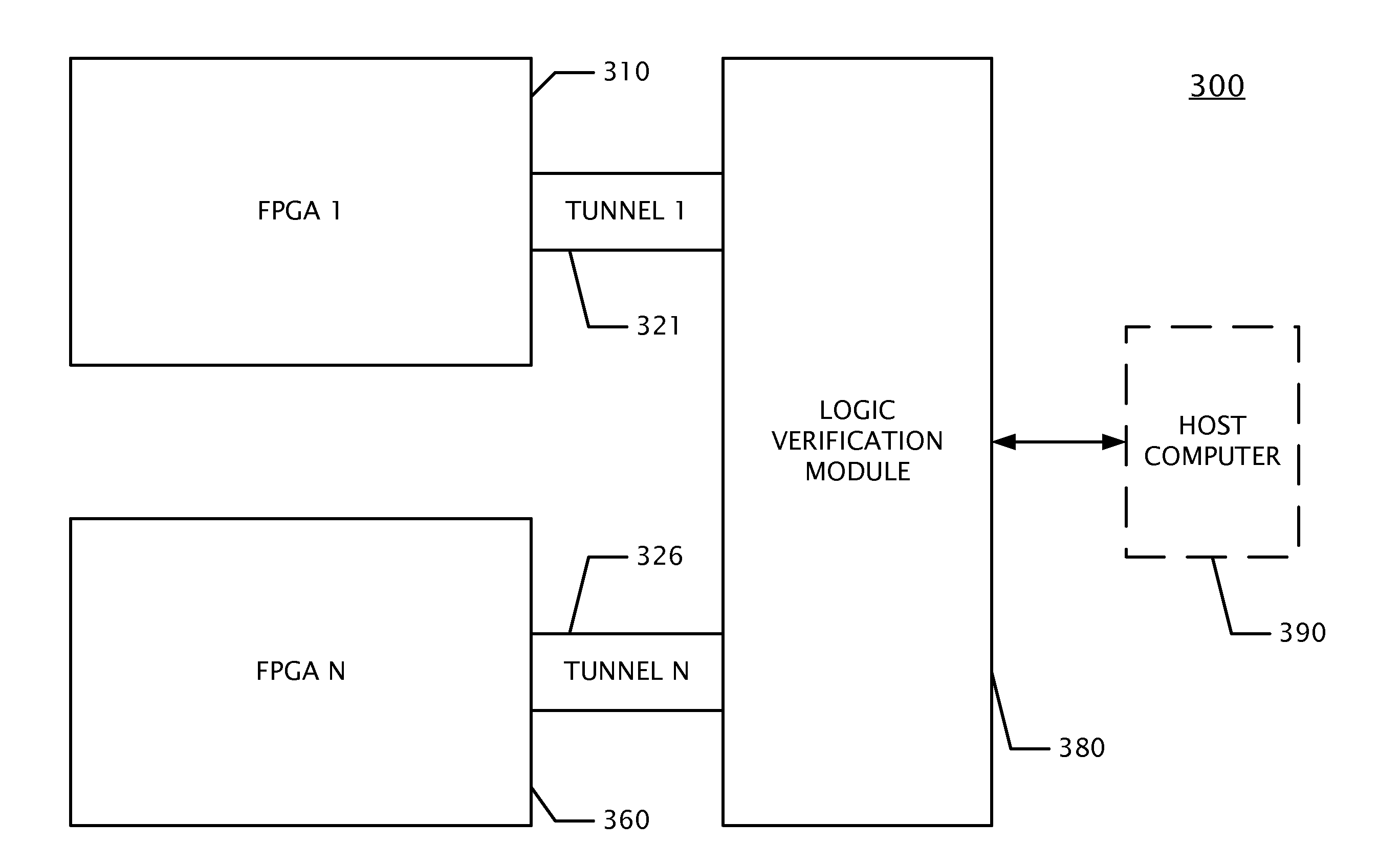
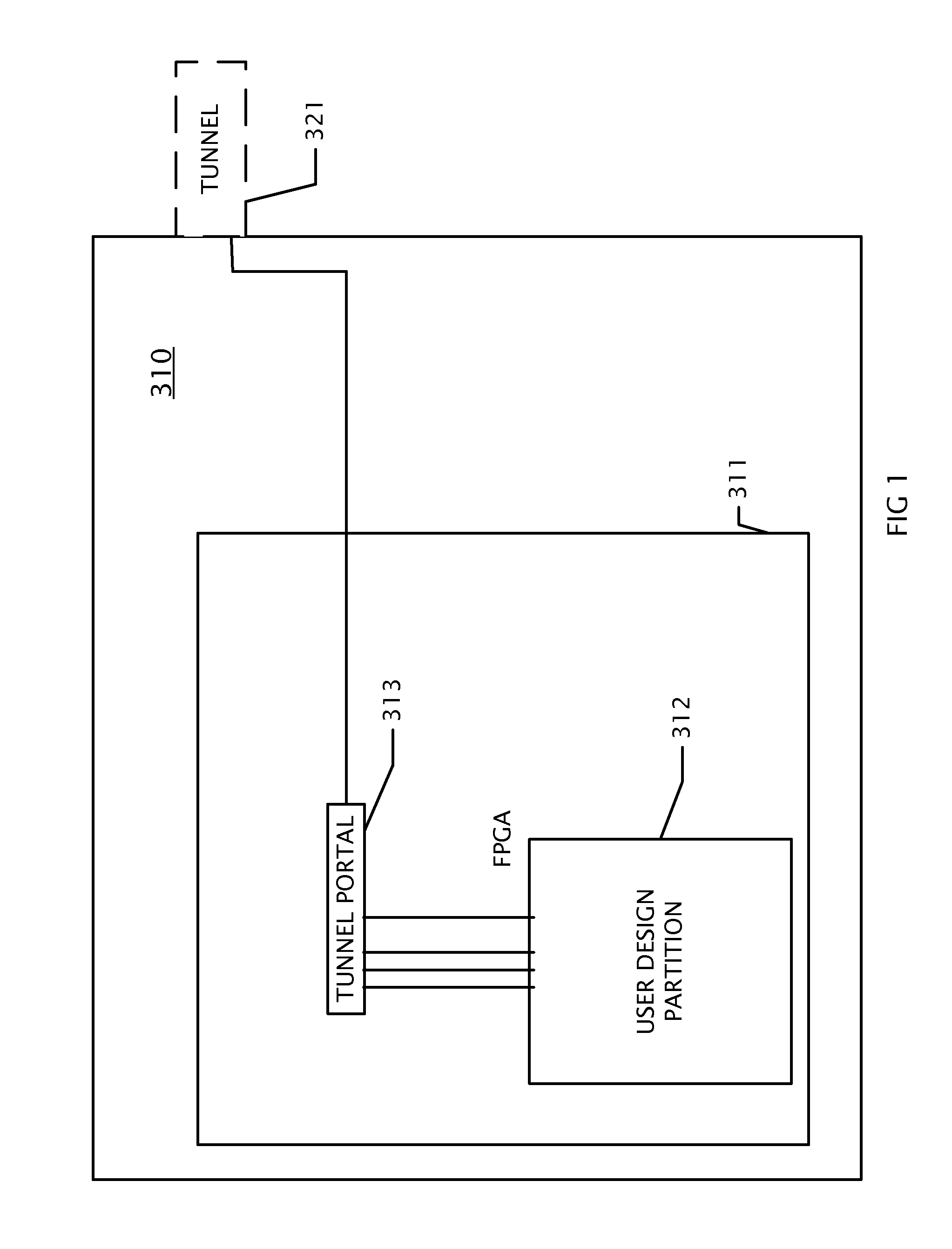
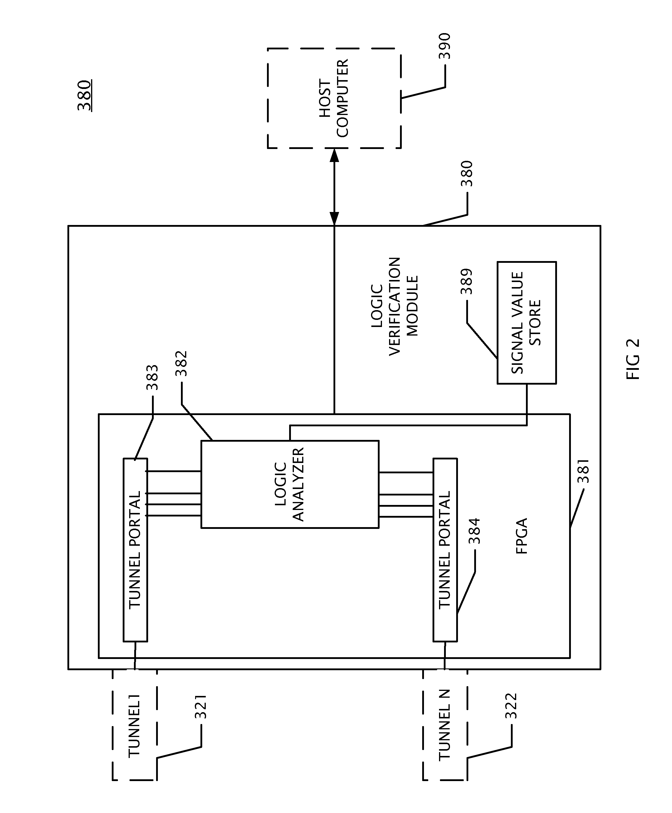
[0026]The present invention provides a method and a system using a reconfigurable platform for designing and emulating a user design. A logic verification module and interface to a host computer is compiled into an FPGA. The signals to be traced by the logic verification module reside within an other FPGA. A logic value tunneling circuit is compiled into each FPGA to enable the logic verification module to trigger on and capture logic values internal to an other FPGA. The present invention may be implemented on a platform including memories and a number of field programmable logic devices, such as programmable gate arrays.

[0027]According to one embodiment of the present invention, using the system for emulating and debugging the user design, a user generates a top-level module including the user design. The user then synthesizes and partitions the user design into partitions each suitable for implementing in one of the programmable logic devices. In addition, each programmable logic...


PUM


Abstract

A apparatus and a system and method to operate the above provide a reconfigurable platform for emulating and debugging a user design which exceeds the capacity of a single field programmable logic device (FPGA). The method and system facilitates design and emulation of a system-on-a-chip type user design. The netlist of a user design may be included with logic value tunneling circuits in an emulation using a platform including a number of field programmable devices. A verification module apparatus provides a hyper prototype for debugging an electronic design that exceeds the capacity of a single FPGA. A verification module provides access to a plurality of attached FPGAs by means of Logic Value Tunneling Transmitters and Receivers which deliver many signals over few pins.

Description

RELATED PATENTS AND APPLICATIONS[0001]This application claims the benefit of provisional patent application Ser. No. 61 / 485,177 submitted on 12 May 2011 by the present inventors, which is incorporated by reference. Priority is claimed from the above provisional application. A related patent is U.S. Pat. No. 7,353,162 “Scalable reconfigurable prototyping system and method.”BACKGROUND[0002]1. Field of the Invention[0003]The present invention relates to automation and validation techniques for designing electronic circuits. In particular, the present invention relates to automation and validation techniques for designing electronic circuits that are particularly applicable to system-on-a-chip type electronic circuits.[0004]2. Description of the Related Art[0005]It is conventional to use field programmable gate array (FPGA) devices from vendors such as Xilinx and Altera to prototype application specific integrated circuits implemented as masked gate arrays or standard cells. However the...

Claims


Application Information

Patent Timeline
Patent Type & Authority Applications(United States)
IPC IPC(8): G06F17/50
CPCG06F17/5045G06F17/5027G06F30/331G06F30/30
Inventor CHENE, MON-REN
Owner S2C LTD
Why Eureka
Try Eureka