

Monolithic metal oxide semiconductor field effect transistor-schottky diode device
- Summary
- Abstract
- Description
- Claims
- Application Information
AI Technical Summary
Benefits of technology
Problems solved by technology
Method used
Image

Examples
Embodiment Construction
[0026]Reference will now be made in detail to the present embodiments of the invention, examples of which are illustrated in the accompanying drawings. Wherever possible, the same reference numbers are used in the drawings and the description to refer to the same or like parts.
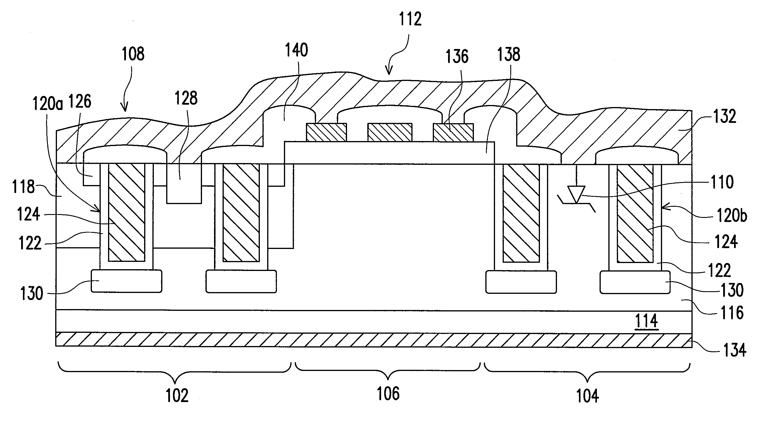
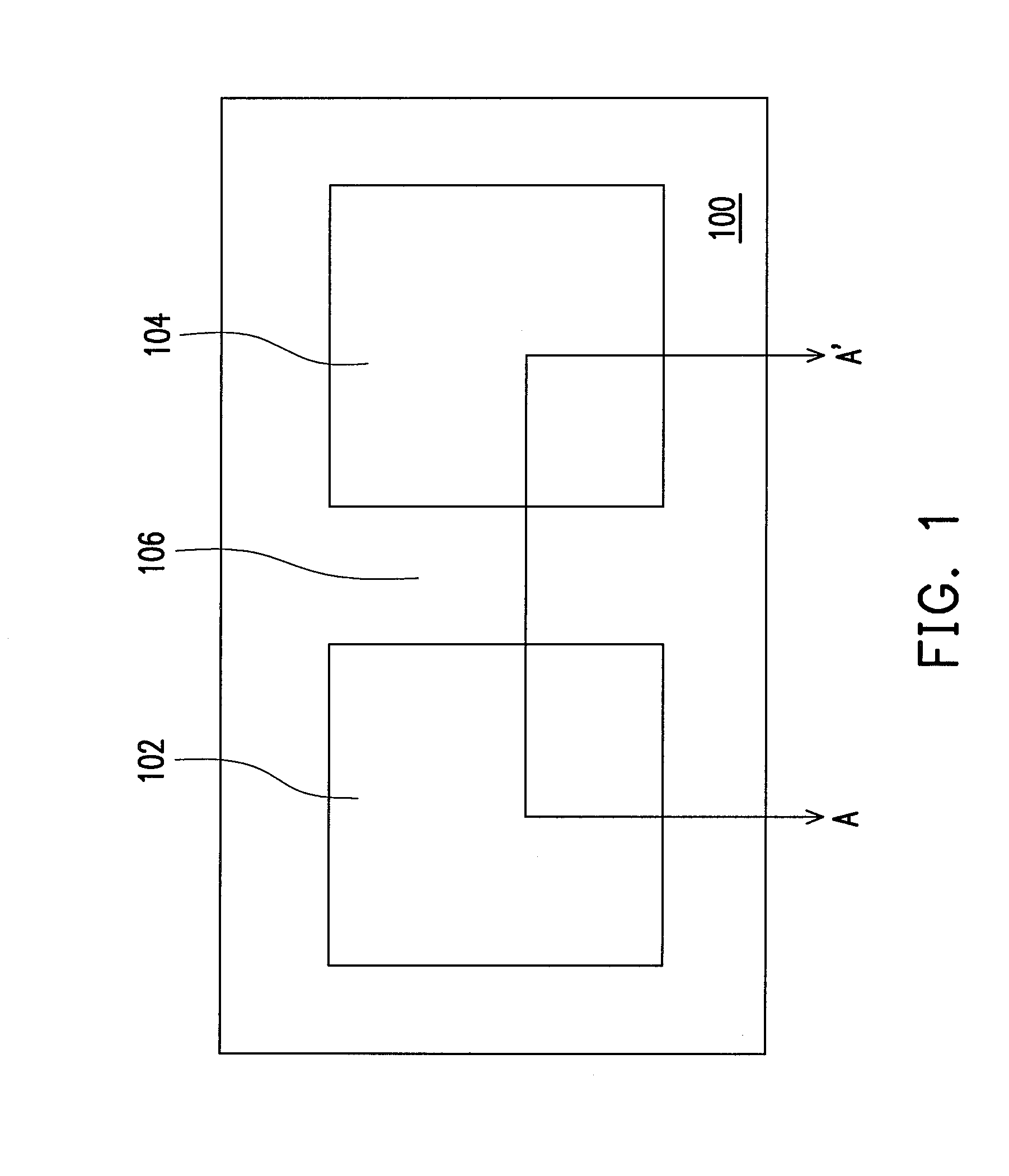
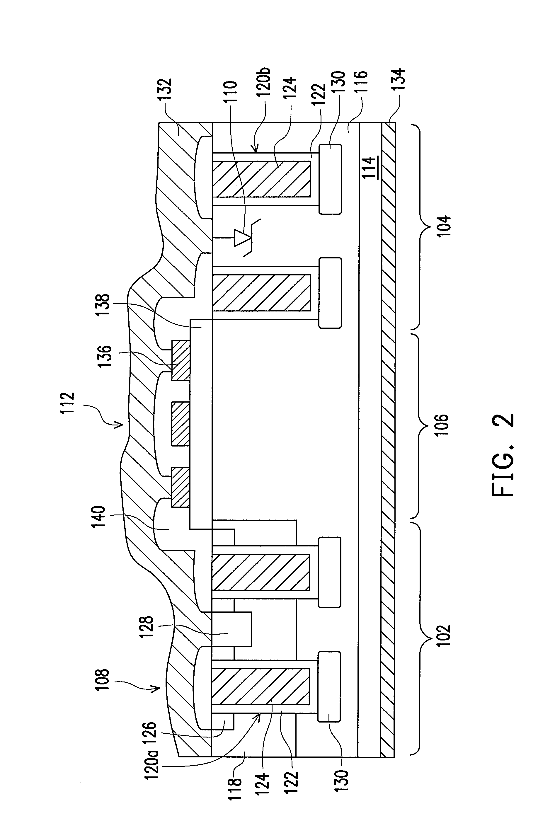
[0027]In a monolithic MOSFET-Schottky diode device according to the present invention, a MOSFET and a Schottky diode are integrated in a single chip; in addition, the MOSFET and the Schottky diode share a termination structure.
[0028]Types of the MOSFET are not limited in the present invention, which may be divided into a flat MOSFET and a trench MOSFET from the perspective of a gate disposing manner; and may be divided into a super junction MOSFET, a dual gate MOSFET and a floating gate MOSFET from the perspective of a design layout manner.
[0029]Types of the Schottky diode are not limited in the present invention, and the Schottky diode may be a junction barrier Schottky diode or a trench Schottky diode.
[0030]...
PUM
 Abstract
Description
Claims
Application Information