Programmable logic device

Active Publication Date: 2012-11-22
SEMICON ENERGY LAB CO LTD
View PDF10 Cites 72 Cited by
  • Summary
  • Abstract
  • Description
  • Claims
  • Application Information

AI Technical Summary

Benefits of technology

[0019]A transistor in a memory portion of a programmable switch includes a wide bandgap semiconductor such as an oxide semiconductor, which allows a sufficient reduction in off-state current of the transistor, whereby configuration data can be held even when a power supply potential is n

Problems solved by technology

However, in a programmable logic device including a volatile memory in a memory portion of a programmable switch, when the supply of power supply potential is stopped, configuration data stored in the memory portion is lost.
Therefore, there is a long delay time from the start of supply of power to operation of the logic block.
In other words, in the programmable logic device including the volatile memory in the memory portion of the programmable switch,

Method used


Image

  • Programmable logic device
  • Programmable logic device
  • Programmable logic device

Examples


Example

Embodiment 1

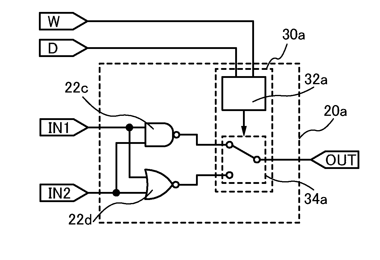
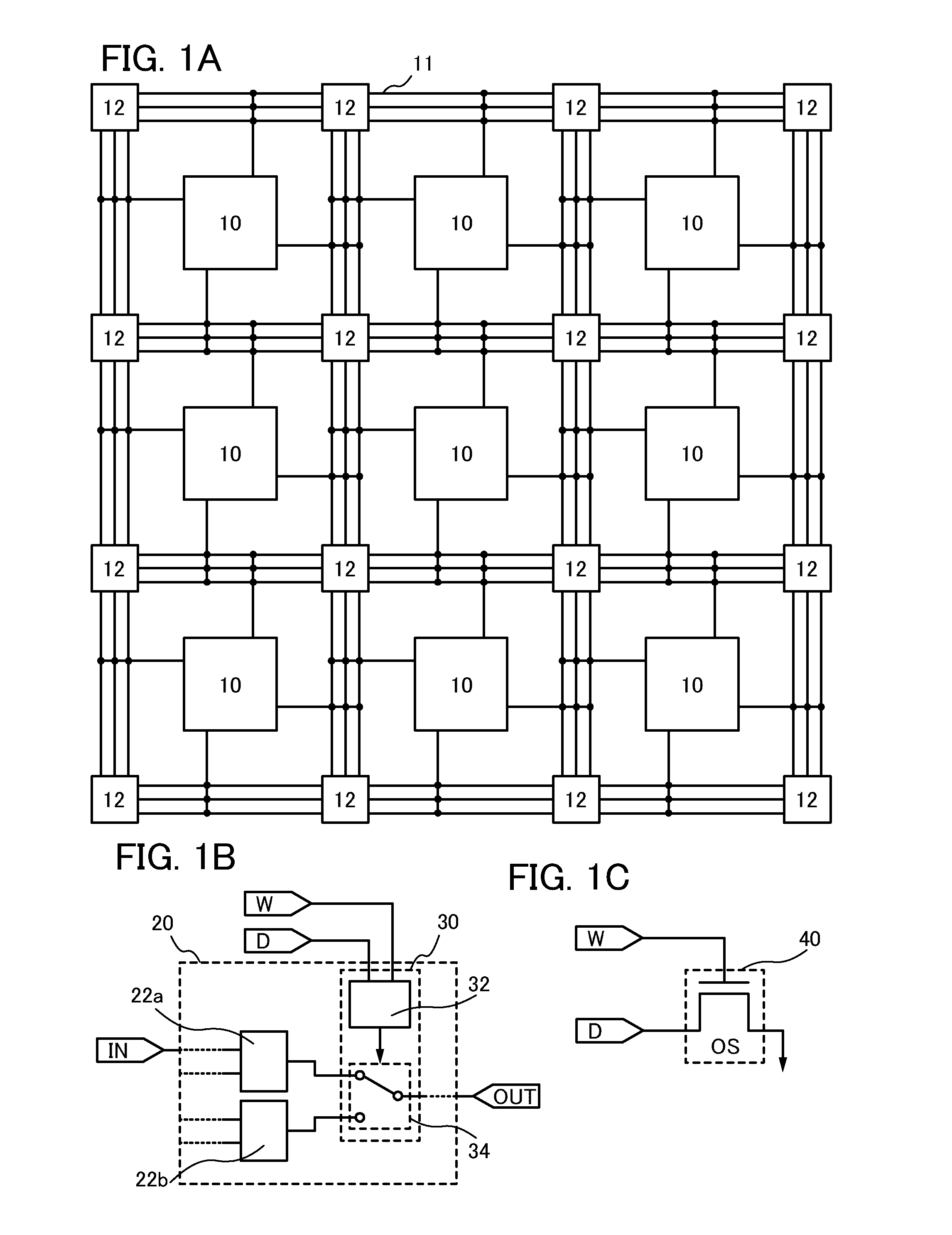
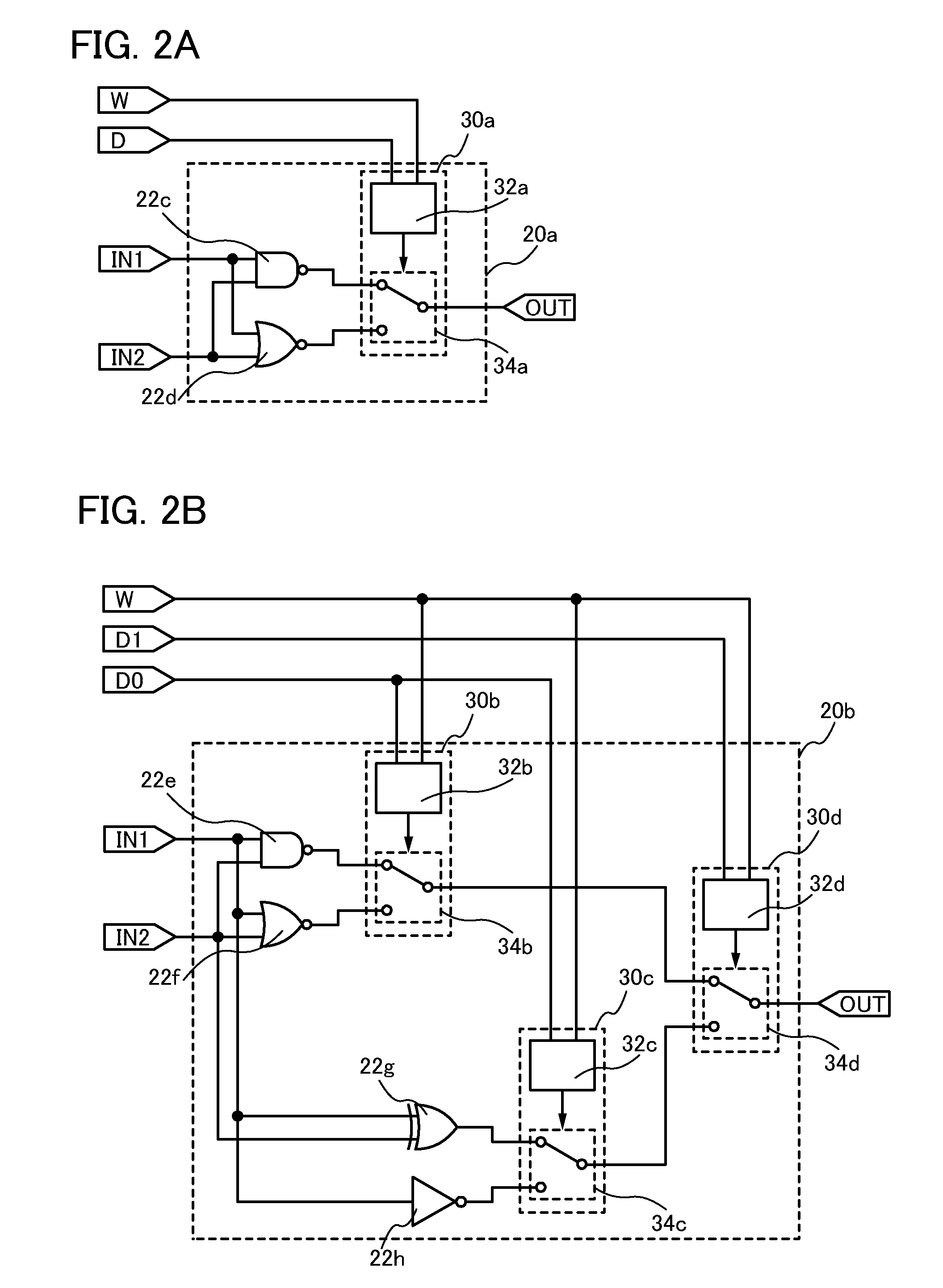
[0056]In this embodiment, a circuit structure of a programmable logic device according to an embodiment of the disclosed invention will be described with reference to FIGS. 1A to 1C, FIGS. 2A and 2B, FIGS. 3A to 3D, FIGS. 4A to 4C, and FIGS. 5A to 5C.

[0057]FIG. 1A illustrates the structure of the programmable logic device according to an embodiment of the disclosed invention. The programmable logic device includes a plurality of logic blocks 10 electrically connected through a plurality of wirings 11. For example, as illustrated in FIG. 1A, the logic blocks 10 are arranged in matrix, and the wirings 11 are provided between the logic blocks 10 to extend in the row direction and in the column direction. Further, a switch matrix 12 for switching connection of the wirings 11 is provided at an intersection of the wirings 11 extending in the row direction and the wirings 11 extending in the column direction. Note that the logic blocks 10 are not necessarily arranged in matrix ...

Example

Embodiment 2

[0102]In this embodiment, a method for manufacturing the programmable switch of the programmable logic device in Embodiment 1 will be described with reference to FIGS. 6A to 6D, FIGS. 7A and 7B, FIGS. 8A to 8C, and FIGS. 9A and 9B. A method for manufacturing the programmable switch including the transistor 110, the transistor 112, and the transistor 114, which is illustrated in FIG. 3A, will be described as an example. Note that in FIGS. 6A to 6D, FIGS. 7A and 7B, FIGS. 8A to 8C, and FIGS. 9A and 9B, a cross-sectional view taken along line A-B corresponds to a cross-sectional view of a region where the transistor 110 including an oxide semiconductor film, the n-channel transistor 112, and the p-channel transistor 114 are formed, and a cross-sectional view taken along line C-D corresponds to a cross-sectional view of the node FG at which the one of the source electrode and the drain electrode of the transistor 110 including an oxide semiconductor layer is connected to the...

Example

Embodiment 3

[0251]In this embodiment, the field-effect mobility of the transistor including an oxide semiconductor film, which is described in the above embodiments, is theoretically calculated, and the transistor characteristics are calculated from the field-effect mobility.

[0252]The actually measured field-effect mobility of an insulated gate transistor can be lower than its ideal mobility because of a variety of reasons; this phenomenon occurs not only in the case of using an oxide semiconductor. One of the reasons that reduce the mobility is a defect inside a semiconductor or a defect at an interface between the semiconductor and an insulating film. When a Levinson model is used, the field-effect mobility on the assumption that no defect exists inside the semiconductor can be calculated theoretically.

[0253]Assuming that the ideal mobility and the measured field-effect mobility of a semiconductor are μ0 and μ, respectively, and a potential barrier (such as a grain boundary) exist...


PUM


Abstract

An object is to provide a programmable logic device which can hold configuration data even when a power supply potential is not supplied, has short start-up time of a logic block after the power is supplied, and can operate with low power. A transistor in a memory portion of a programmable switch includes a material which allows a sufficient reduction in off-state current of the transistor, such as an oxide semiconductor material which is a wide bandgap semiconductor. When the semiconductor material which allows a sufficient reduction in off-state current of the transistor is used, configuration data can be held even when a power supply potential is not supplied.

Description

TECHNICAL FIELD[0001]The present invention relates to a programmable logic device and a semiconductor device including the programmable logic device. Further, the present invention relates to an electronic device including the semiconductor device.BACKGROUND ART[0002]In general, a circuit structure of a semiconductor integrated circuit typified by an integrated circuit (IC) or a large scale integrated circuit (LSI) is fixed at the time of manufacture and cannot be changed after the manufacture. In contrast, a semiconductor integrated circuit called a programmable logic device (PLD) has a structure in which unit logic blocks each including a plurality of logic circuits are electrically connected to each other through wirings. In the programmable logic device, a circuit structure of each logic block can be controlled by an electric signal.[0003]Accordingly, the design of the programmable logic device can be changed even after the manufacture. Thus, time and cost required for designing...

Claims


Application Information

Patent Timeline
IPC IPC(8): H03K19/177H01L29/94
CPCH03K19/1776H03K19/17764H01L27/1225H01L27/0688H01L27/11803H03K19/17772H03K19/17736H03K19/17728
Inventor NISHIJIMA, TATSUJIYONEDA, SEIICHI
Owner SEMICON ENERGY LAB CO LTD
Why Eureka
Try Eureka