Programmable logic device

a programmable logic and semiconductor technology, applied in the direction of power consumption reduction, pulse technique, instruments, etc., can solve the problems of long delay time, loss of configuration data stored in the memory portion, and difficulty in performing normal-off driving methods in which supply of power supply potential is temporarily stopped, so as to reduce the power consumption the start-up time of a programmable logic device can be short, and the off-state current is sufficiently reduced.

Inactive Publication Date: 2012-11-22
SEMICON ENERGY LAB CO LTD
View PDF6 Cites 56 Cited by
  • Summary
  • Abstract
  • Description
  • Claims
  • Application Information

AI Technical Summary

Benefits of technology

[0009]In the case where a non-volatile memory, which has a floating gate transistor, is used in a memory portion of a programmable switch for controlling connection of wirings between logic blocks in a programmable logic device, configuration data can be held even when power supply potential is not supplied temporarily by a normally-off driving method. However, a high potential is needed because electrons are injected into a floating gate in data writing; accordingly, a long time is required to write data. Moreover, a gate insulating layer of the floating gate readily deteriorates because of tunneling current in the data writing.
[0010]In view of the above problems, it is an object to provide a programmable logic device which can hold configuration data even when a power supply potential is not supplied, has short start-up time after the power is supplied, and can operate with low power.
[0018]A transistor in a memory portion of a programmable switch for controlling connection of wirings between logic blocks includes a wide bandgap semiconductor such as an oxide semiconductor, which allows a sufficient reduction in off-state current of the transistor, whereby configuration data can be held even when a power supply potential is not supplied. With such a structure, writing of configuration data after the power is supplied can be omitted, so that start-up time of a programmable logic device can be short. Accordingly, a reduction in power consumption of a programmable logic device can be achieved by a normally-off driving method.

Problems solved by technology

However, in a programmable logic device including a volatile memory in a memory portion of a programmable switch for controlling connection of wirings between logic blocks, when the supply of power supply potential is stopped, configuration data stored in the memory portion is lost.
Therefore, there is a long delay time from the start of supply of power to operation of the programmable logic device.
In other words, in the programmable logic device including the volatile memory in the memory portion of the programmable switch, it is difficult to perform a normally-off driving method in which supply of power supply potential is temporarily stopped.
However, a high potential is needed because electrons are injected into a floating gate in data writing; accordingly, a long time is required to write data.
Moreover, a gate insulating layer of the floating gate readily deteriorates because of tunneling current in the data writing.

Method used


Image

  • Programmable logic device
  • Programmable logic device
  • Programmable logic device

Examples


embodiment 1

[0056]In this embodiment, a circuit structure of a programmable logic device according to an embodiment of the disclosed invention will be described with reference to FIGS. 1A and 1B, FIGS. 2A to 2C, FIGS. 3A to 3D, FIGS. 4A to 4C, and FIGS. 5A to 5C.

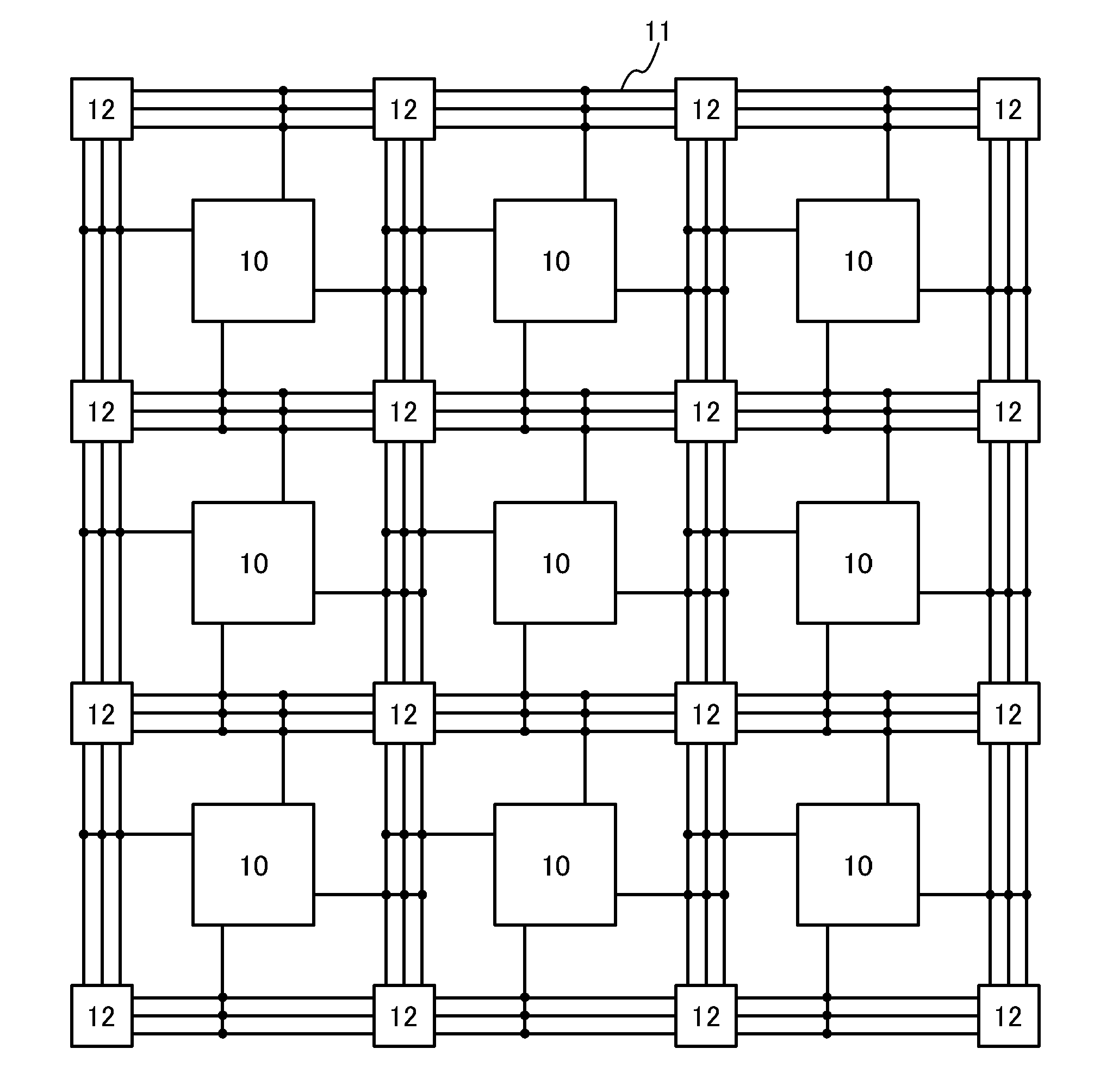
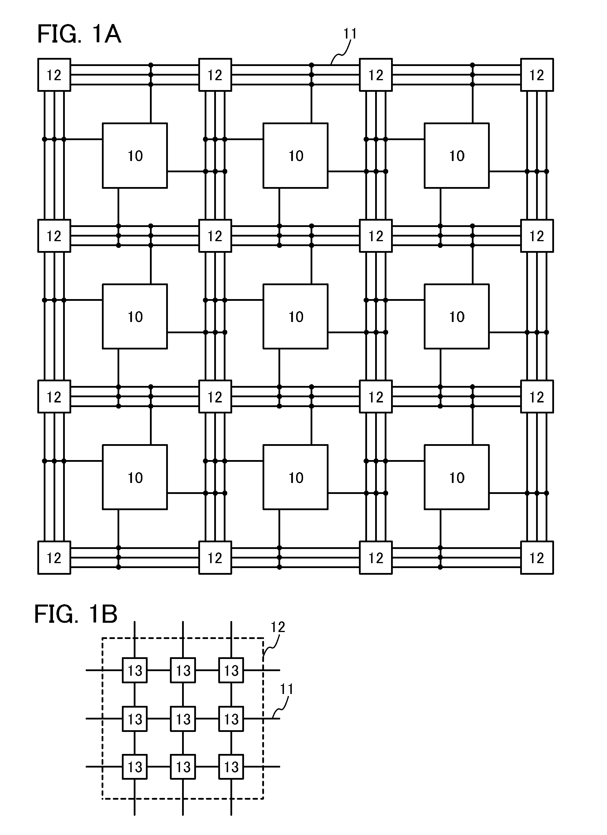
[0057]FIG. 1A shows a structure of a programmable logic device according to an embodiment of the disclosed invention. The programmable logic device includes a plurality of logic blocks 10 each including a plurality of logic circuits, a plurality of wirings 11 electrically connected to the plurality of logic blocks 10, and switch matrixes 12 each provided at an intersection of the plurality of wirings 11. The plurality of logic blocks 10 is preferably arranged in matrix as illustrated in FIG. 1A. At least one wiring 11 is provided between the logic blocks 10 and extends in the row direction or in the column direction. Further, each of the switch matrixes 12 is provided at the intersection of the plurality of wirings 11 extending in the r...

embodiment 2

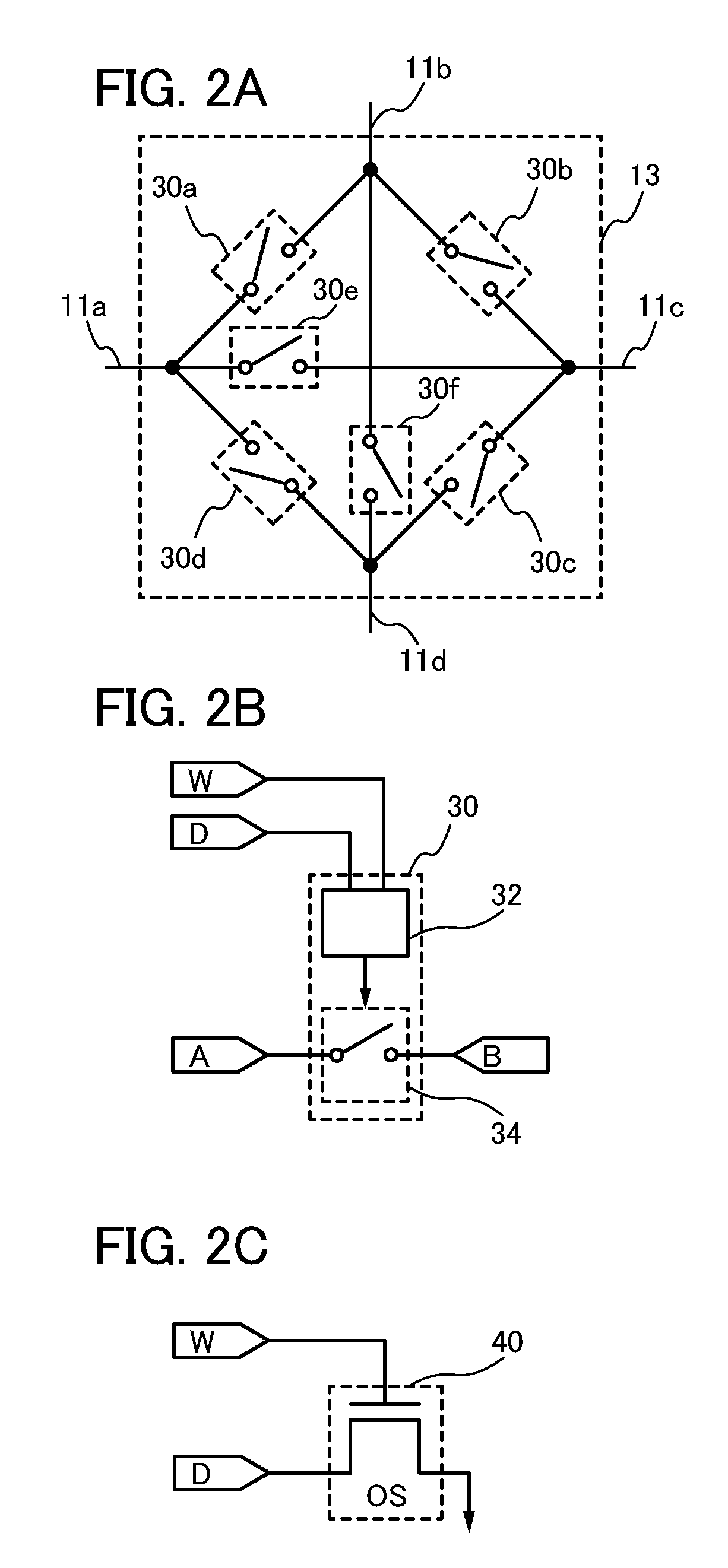
[0108]In this embodiment, a method for manufacturing the programmable switch of the programmable logic device in Embodiment 1 will be described with reference to FIGS. 6A to 6D, FIGS. 7A and 7B, FIGS. 8A to 8C, and FIGS. 9A and 9B. A method for manufacturing the programmable switch including the transistor 110 and the transistor 112, which is illustrated in FIG. 3A, will be described as an example. Note that in FIGS. 6A to 6D, FIGS. 7A and 7B, FIGS. 8A to 8C, and FIGS. 9A and 9B, a cross-sectional view taken along line A-B corresponds to a cross-sectional view of a region where the transistor 110 including an oxide semiconductor film and the n-channel transistor 112 are formed, and a cross-sectional view taken along line C-D corresponds to a cross-sectional view of the node FG at which the one of the source electrode and the drain electrode of the transistor 110 including an oxide semiconductor film is connected to the gate electrode of the n-channel transistor 112.

[0109]First, as i...

embodiment 3

[0263]In this embodiment, the field-effect mobility of the transistor including an oxide semiconductor film, which is described in the above embodiments, is theoretically calculated, and the transistor characteristics are calculated from the field-effect mobility.

[0264]The actually measured field-effect mobility of an insulated gate transistor is lower than its theoretical mobility because of a variety of reasons; this phenomenon occurs not only in the case of using an oxide semiconductor. One of the reasons that reduce the mobility is a defect inside a semiconductor or a defect at an interface between the semiconductor and an insulating film. When a Levinson model is used, the field-effect mobility on the assumption that no defect exists inside the semiconductor can be calculated theoretically.

[0265]Assuming that a potential barrier (such as a grain boundary) exists in the semiconductor, the measured field-effect mobility μ can be expressed by the following Formula 2.

[Formula2]μ=μ0...


PUM


Abstract

An object is to provide a programmable logic device having logic blocks connected to each other by a programmable switch, where the programmable switch is characterized by an oxide semiconductor transistor incorporated therein. The extremely low off-state current of the oxide semiconductor transistor provides a function as a non-volatile memory due to its high ability to hold a potential of a gate electrode of a transistor which is connected to the oxide semiconductor transistor. The ability of the oxide semiconductor transistor to function as a non-volatile memory allows the configuration data for controlling the connection of the logic blocks to be maintained even in the absence of a power supply potential. Hence, the rewriting process of the configuration data at starting of the device can be omitted, which contributes to the reduction in power consumption of the device.

Description

TECHNICAL FIELD[0001]The present invention relates to a programmable logic device and a semiconductor device including the programmable logic device. Further, the present invention relates to an electronic device including the semiconductor device.BACKGROUND ART[0002]In general, a circuit structure of a semiconductor integrated circuit typified by an integrated circuit (IC) or a large scale integrated circuit (LSI) is fixed at the time of manufacture and cannot be changed after the manufacture. In contrast, a semiconductor integrated circuit called a programmable logic device (PLD) has a structure in which unit logic blocks each including a plurality of logic circuits are electrically connected to each other through wirings. In the programmable logic device, a circuit structure of each logic block can be controlled by an electric signal.[0003]Accordingly, the design of the programmable logic device can be changed even after the manufacture. Thus, time and cost required for designing...

Claims


Application Information

Patent Timeline
Patent Type & Authority Applications(United States)
IPC IPC(8): H03K19/00
CPCH03K19/17736H03K19/0008H03K19/17744H03K19/0013H03K19/177H01L27/1225H01L27/124H01L29/7869
Inventor YONEDA, SEIICHINISHIJIMA, TATSUJI
Owner SEMICON ENERGY LAB CO LTD
Why Eureka
Try Eureka