Shift register unit circuit, shift register, array substrate and liquid crystal display

Active Publication Date: 2012-11-22
BOE TECH GRP CO LTD +1
View PDF13 Cites 53 Cited by
  • Summary
  • Abstract
  • Description
  • Claims
  • Application Information

AI Technical Summary

Benefits of technology

[0043]a) By using a design of double level pulling-down, the pulling-down for a TFT changes to an Alternating Current pulling-down from a Direct Current pulling-down, thus the problem that the threshold voltage of the pulling-down TFT would drift under the direct current bias voltage is settled, and in turn the TFT AC Duty Cycle is reduced.
[0044]b) Suspensions in

Problems solved by technology

However, in prior art, the shift register unit circuit formed by the transistors of TFT same different-electricity type has problems that a threshold voltage of pulling-down T

Method used


Image

  • Shift register unit circuit, shift register, array substrate and liquid crystal display
  • Shift register unit circuit, shift register, array substrate and liquid crystal display
  • Shift register unit circuit, shift register, array substrate and liquid crystal display

Examples


embodiment 1

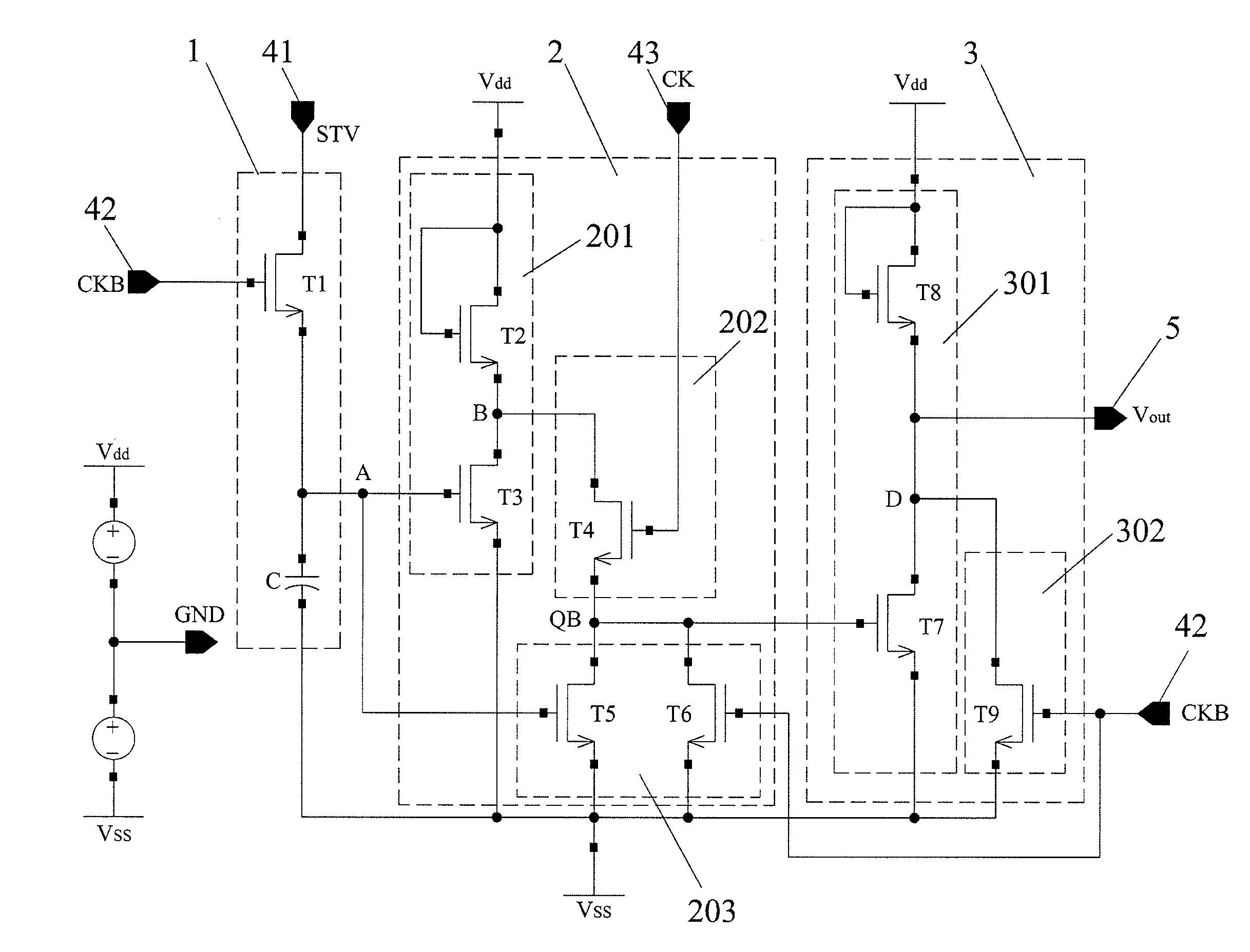
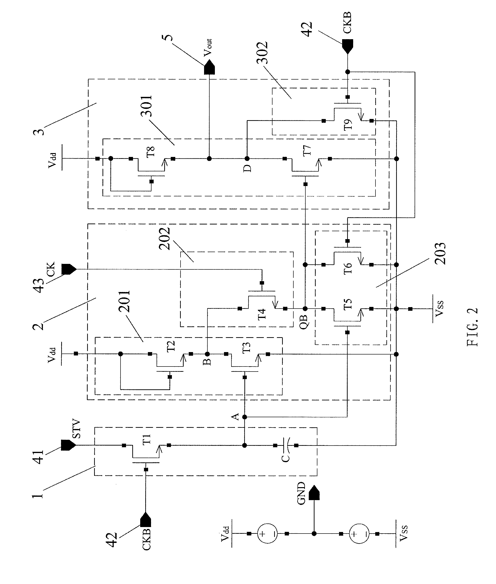
[0065]FIG. 2 illustrates a shift register unit circuit according to an embodiment of the disclosed technical solution, and all of switches T1-T9 in this embodiment are TFTs (Thin Film Transistor). As can be seen from the figure, the pre-charging circuit 1 comprises a first switch T1, a first node A and a capacitor C. A gate of the first switch T1 is connected to a first clock signal CKB, a drain thereof is connected to a start signal (the start signal may be a STV signal or a level signal output from the shift register unit circuit in the previous stage), and the source thereof is coupled to the first node A; the first node A is a turn-on level output terminal of the pre-charging circuit 1; and one terminal of the capacitor C is coupled to the first node A, and the other terminal is coupled to a low level VSS.

[0066]The first level pulling-down circuit 2 comprises a first inverting circuit 201, a level pulling-up circuit 202 and a first level pulling-down sub-circuit 203. The first i...

embodiment 2

[0077]FIG. 3 illustrates a shift register unit circuit according to another embodiment of the disclosed technical solution. This embodiment only changes the gate of the fifth switch T5 in the Embodiment 1 as being coupled to the output terminal of the second level pulling-down circuit. Since the timing diagram of the level outputted at the node A is the same as that of the scan signal output terminal Vout after time t2, the effects on the T5 are the same, that is, the operation principle of this embodiment is the same as the Embodiment 1.

[0078]As shown in FIG. 5, the shift register comprises multiple stages of the shift register units S1, S2, . . . , Sn, wherein respective stages of the shift register units generate their scan signals at respective output terminals (OUT0, OUT1, OUT2, . . . , OUTn). The shift register unit at each stage has a first clock input port CKB, a second clock input port CK, a start signal input port, a reset signal input port RT and a scan signal output port...


PUM


Abstract

Embodiments of the disclosed technical solution provides a shift register unit circuit which operates based on two clock signals and comprises input terminals, a pre-charging circuit, a first level pulling-down circuit, a second level pulling-down circuit and a scan signal output terminal. Embodiments of the disclosed technical solution also provides a shift register having at least two shift register unit circuits connected in cascade, and further provides a liquid crystal display array substrate and a liquid crystal display. Embodiments of the disclosed technical solution settles problems that a threshold voltage of the pulling-down TFT would drift under a direct current bias voltage and a output is unstable due to a clock hopping, increases a reliability of the circuit and reduces power consumption.

Description

BACKGROUND[0001]A disclosed technical solution relates to a shift register unit circuit, a shift register, an array substrate and a liquid crystal display.[0002]The liquid crystal display is a plane display which employs glass substrate as the substrate, and forms color film structure and TFT circuit structure on the glass substrate. In order not to increase any process and manufacture cost, a manufacture process for forming TFTs (Thin Film Transistor) in a pixel circuit is employed to manufacture a driving circuit to make the pixel circuit and the driving circuit on a same substrate only by designing a GOA circuit (for example, a principle view of the shift register unit circuit in the GOA circuit as shown in FIG. 1). In this case, a best scenario is to use transistors of TFT same different-electricity type to form the driving circuit including the shift register so as to reduce the manufacture costs. However, in prior art, the shift register unit circuit formed by the transistors ...

Claims


Application Information

Patent Timeline
IPC IPC(8): G11C19/00G09G3/36
CPCG11C19/184G11C19/28G09G2310/0286G09G2300/0408G09G3/3677
Inventor LI, TIANMAQI, XIAOJINGQING, HAIGANG
Owner BOE TECH GRP CO LTD
Why Eureka
Try Eureka