Arrays of long nanostructures in semiconductor materials and methods thereof

a nanostructure and semiconductor technology, applied in the field of nanostructures, can solve the problems of limited commercial application of thermoelectrics, poor cost performance of these devices, and the limited range of thermoelectrics, and achieve the effect of reducing the cost of thermoelectrics

Inactive Publication Date: 2012-11-22
ALPHABET ENERGY +1
View PDF3 Cites 42 Cited by
  • Summary
  • Abstract
  • Description
  • Claims
  • Application Information

AI Technical Summary

Benefits of technology

[0016]According to yet another embodiment, the method for forming an array of nanowires includes: providing a semiconductor substrate including a first surface and one or more second surfaces; masking at least one or more portions of the one or more second surfaces with at least a first portion of the first surface being exposed; applying a metalized film to at least the exposed first portion of the first surface; etching the semiconductor substrate through at least the exposed first portion of the first surface using a first etchant solution; and forming a first plurality of nanowires. Each of the first plurality of nanowires includes a first end at a third surface an

Problems solved by technology

To date, thermoelectrics have had limited commercial applicability due to the poor cost performance of these devices compared to other technologies that accomplish similar means of energy generation or refrigeration.
Where other technologies usually are not as suitable as thermoelectrics for use in lightweight and low footprint applications, thermoelectrics often have nonetheless been limited by their prohibitively high costs.
The thermoelectric materials in presently available commercial thermoelectric modules are generally comprised of bismuth telluride or lead telluride, which are both toxic, difficult to manufacture with, and expen

Method used


Image

  • Arrays of long nanostructures in semiconductor materials and methods thereof
  • Arrays of long nanostructures in semiconductor materials and methods thereof
  • Arrays of long nanostructures in semiconductor materials and methods thereof

Examples


Embodiment Construction

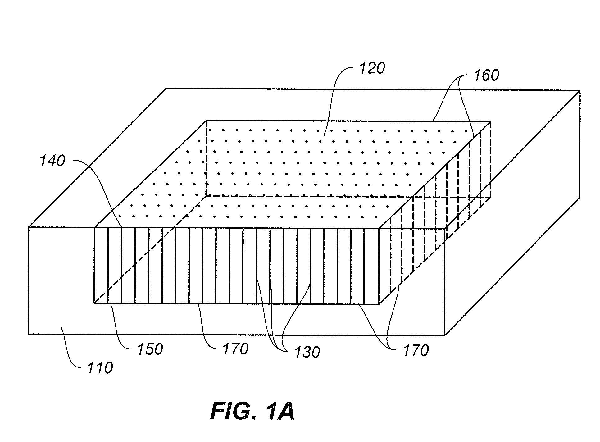
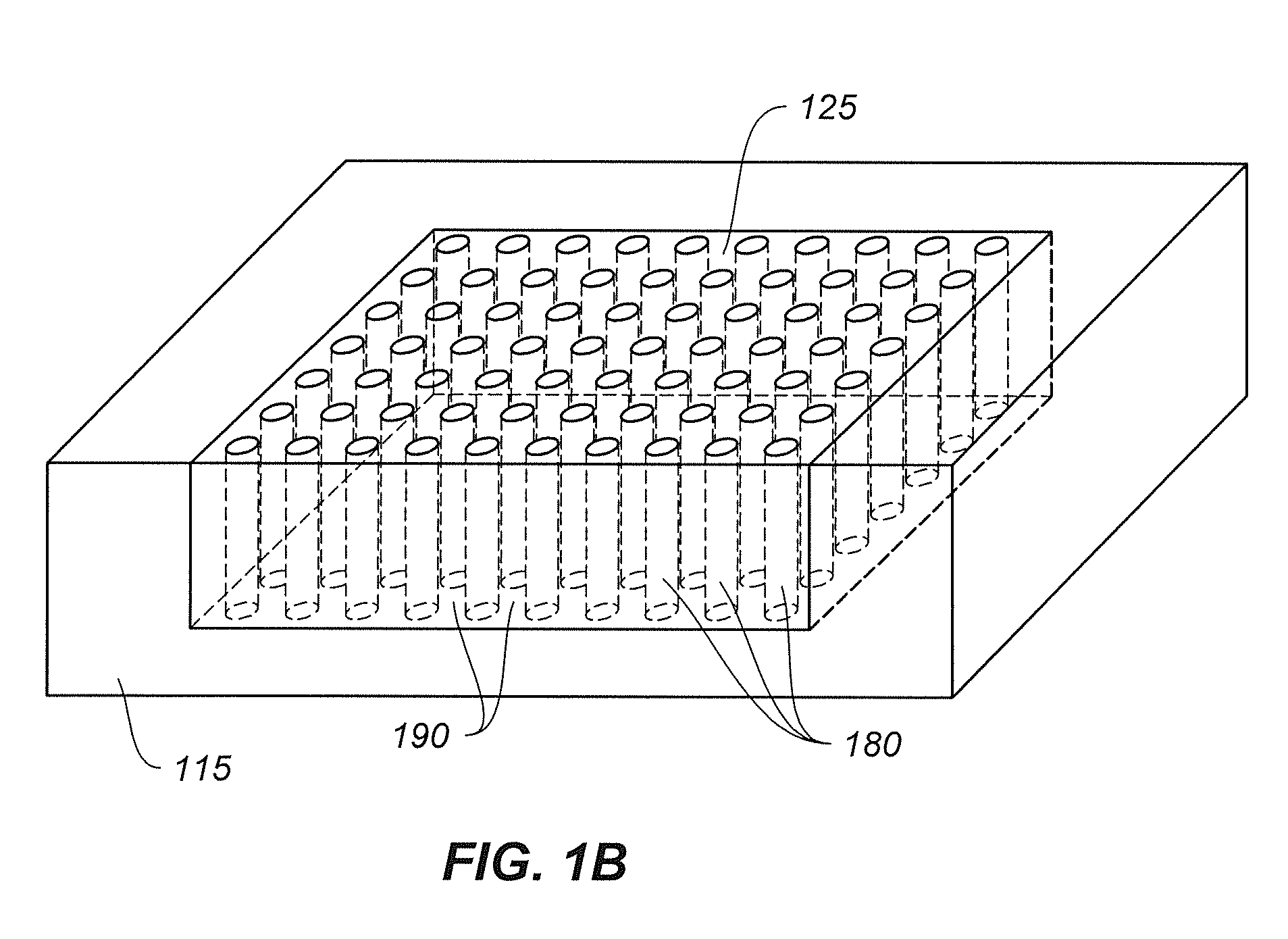
[0036]The present invention is directed to nanostructures. More particularly, the invention provides arrays of long nanostructures in semiconductor substrates and methods thereof. Merely by way of example, the invention has been applied to arrays of long nanowires in silicon with certain thermoelectric properties. However, it would be recognized that the invention has a much broader range of applicability, including but not limited to use in solar power, battery electrodes and / or energy storage, catalysis, and / or light emitting diodes.

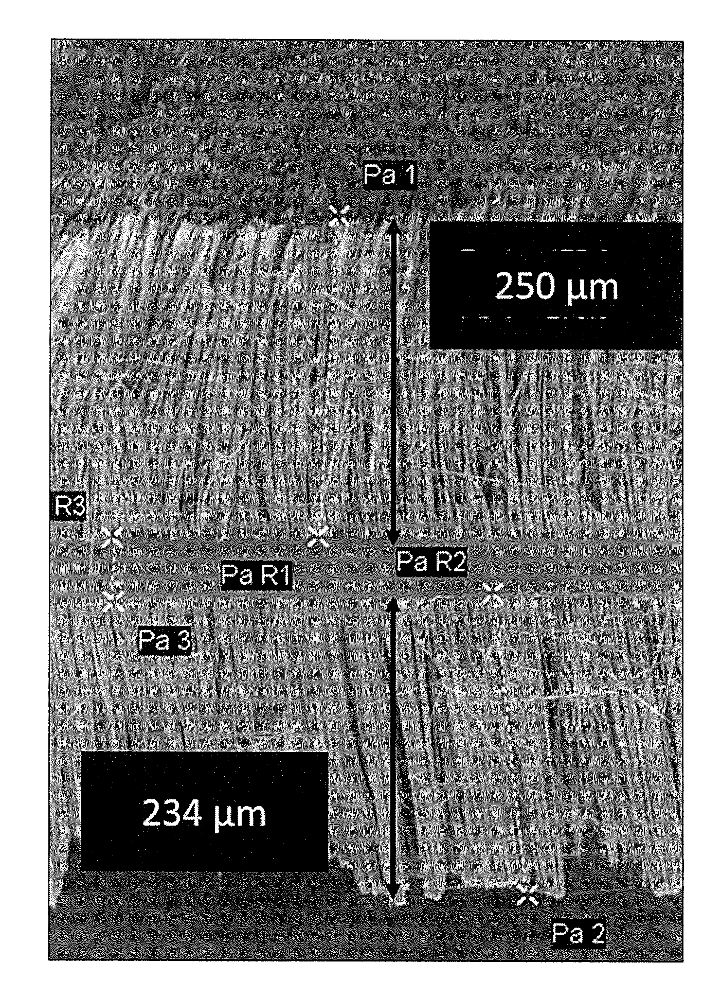
[0037]In general, the usefulness of a thermoelectric material depends upon the physical geometry of the material. For example, the larger the surface area of the thermoelectric material that is presented on the hot and cold sides of a thermoelectric device, the greater the ability of the thermoelectric device to support heat and / or energy transfer through an increase in power density. In another example, a suitable minimum distance (i.e., the length of...


PUM

PropertyMeasurementUnit
Lengthaaaaaaaaaa
Areaaaaaaaaaaa
Areaaaaaaaaaaa

Abstract

An array of nanowires and method thereof. The array of nanowires includes a plurality of nanowires. The plurality of nanowires includes a plurality of first ends and a plurality of second ends respectively. For each of the plurality of nanowires, a corresponding first end selected from the plurality of first ends and a corresponding second end selected from the plurality of second ends are separated by a distance of at least 200 μm. All nanowires of the plurality of nanowires are substantially parallel to each other.

Description

CROSS-REFERENCES TO RELATED APPLICATIONS[0001]This application claims priority to U.S. Provisional Application No. 61 / 415,577, filed Nov. 19, 2010, commonly assigned and incorporated by reference herein for all purposes.STATEMENT AS TO RIGHTS TO INVENTIONS MADE UNDER FEDERALLY SPONSORED RESEARCH OR DEVELOPMENT[0002]Work described herein has been supported, in part, by U.S. Air Force SBIR Contract No. FA8650-10-M-2031. The United States Government may therefore have certain rights in the invention.BACKGROUND OF THE INVENTION[0003]The present invention is directed to nanostructures. More particularly, the invention provides arrays of long nanostructures in semiconductor substrates and methods thereof. Merely by way of example, the invention has been applied to arrays of long nanowires in silicon with certain thermoelectric properties. However, it would be recognized that the invention has a much broader range of applicability, including but not limited to use in solar power, battery e...

Claims


Application Information

Patent Timeline
IPC IPC(8): B32B3/14H01L21/308D02G3/22H01L29/06
CPCB82Y30/00Y10T428/24802Y10T428/2913B82Y40/00H01L21/3081B82Y10/00H01L29/0676Y10T428/249924H10N19/00H10N10/80H10N10/01H01L21/3085H01L21/3086H01L31/035227
Inventor YI, MINGQIANGSCULLIN, MATTHEW L.MATUS, GABRIEL ALEJANDROHILKEN, DAWN L.LEE, CHII GUANGMUCKENHIRN, SYLVAIN
Owner ALPHABET ENERGY
Why Eureka
Try Eureka