Voltage controlled switching element gate drive circuit
- Summary
- Abstract
- Description
- Claims
- Application Information
AI Technical Summary
Benefits of technology
Problems solved by technology
Method used
Image
Examples
first embodiment
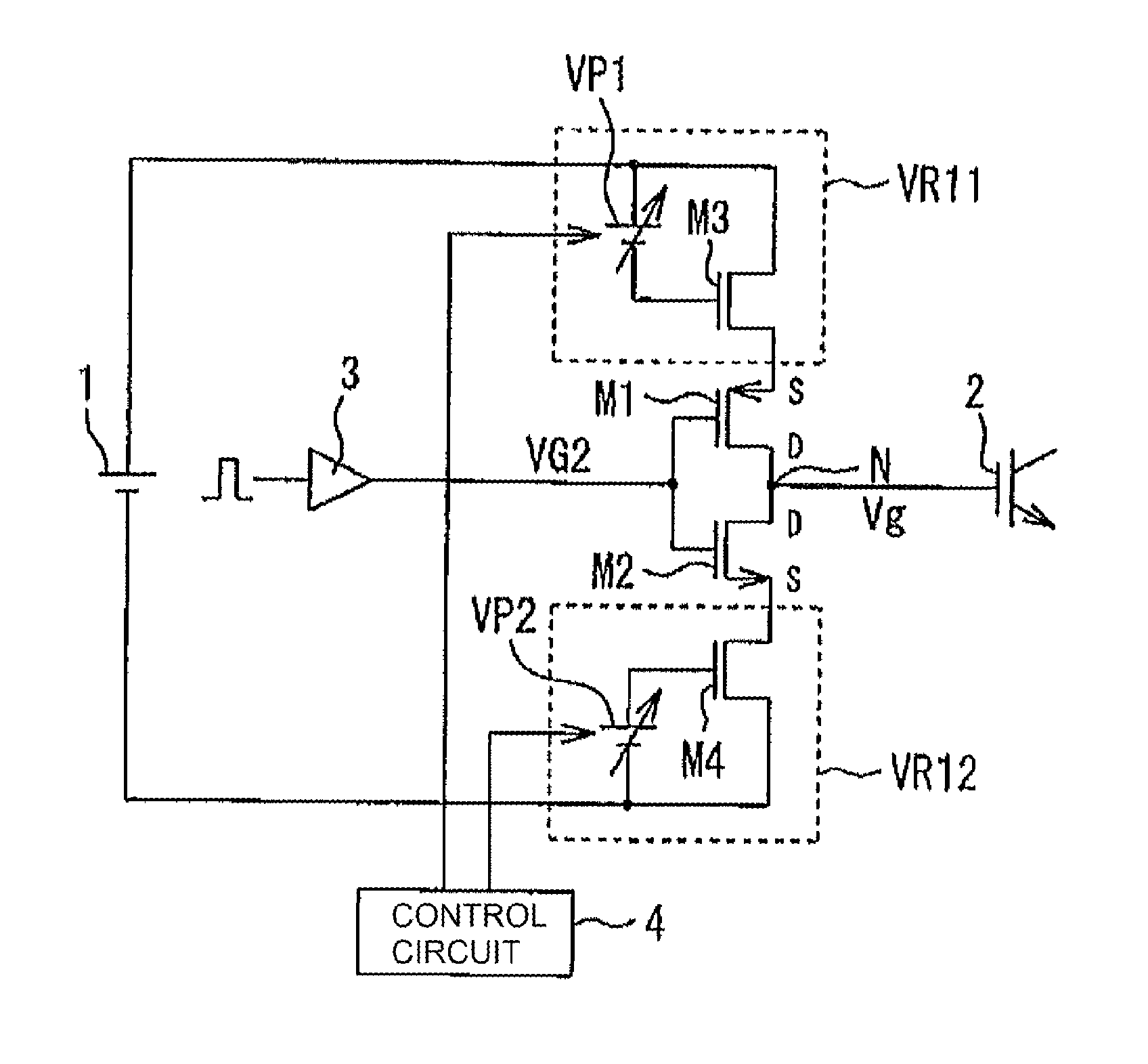
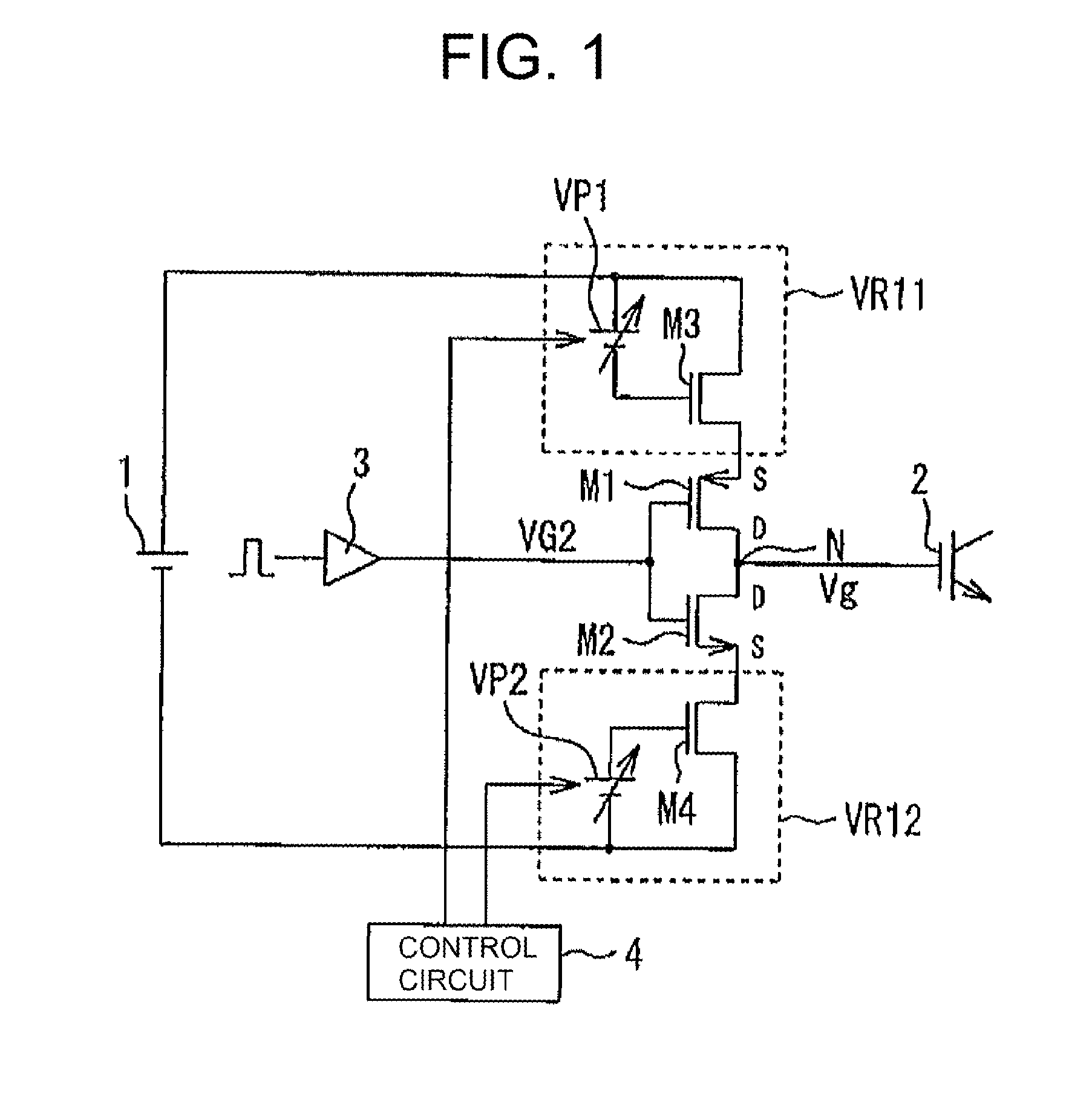
[0043]FIG. 1 is a circuit diagram showing a voltage controlled switching element gate drive circuit according to the invention. In FIG. 1, the gate drive circuit has a direct current power source 1, and the source of a PMOS field effect transistor M1 is connected via a first variable resistor VR11 to the positive electrode side of the direct current power source 1.
[0044]The drain of the PMOS field effect transistor M1 is connected to the drain of an NMOS field effect transistor M2, and the source of the NMOS field effect transistor M2 is connected to the negative electrode side of the direct current power source 1 via a first variable resistor VR12.
[0045]Then, a node N, which is a connection point of the drain of the PMOS field effect transistor M1 and the drain of the NMOS field effect transistor M2, is connected to the gate of an insulated gate bipolar transistor (hereafter called an IGBT) 2 acting as a voltage controlled switching element that forms a control target.
[0046]Further...
second embodiment
[0082]Next, a description will be given, referring to FIG. 12, of the invention.
[0083]In the second embodiment, instead of a case of configuring a variable resistor by changing the output resistance of an MOS field effect transistor, a variable resistor is configured of plural resistors.
[0084]That is, in the second embodiment, the variable resistors VR11 and VR12 are configured of one or plural parallel circuits PC3 of a resistor R6 and a switch SW3 configured of, for example, a semiconductor switching element, connected in series (in the case of one, there are two kinds of resistance value, 0 and R6), as shown in FIG. 12. Then, the switch SW3 of each parallel circuit PC3 is on-off controlled by the control circuit 4.
[0085]According to the second embodiment too, it is possible to set the minimum resistance value Rmin and maximum value Rmax by on-off controlling the switches SW3 of the parallel circuits PC3 configuring the variable resistors VR11 and VR12 with the control circuit 4 h...
PUM
 Abstract
Description
Claims
Application Information


