Copper nanoparticle application processes for low temperature printable, flexible/conformal electronics and antennas

a technology of flexible/conformal electronics and copper nanoparticles, applied in the field of printed electronics, can solve the problem of limited minimum separation distance of traces, and achieve the effect of small separation distan

Active Publication Date: 2012-12-06
KUPRION INC
View PDF4 Cites 9 Cited by
  • Summary
  • Abstract
  • Description
  • Claims
  • Application Information

AI Technical Summary

Benefits of technology

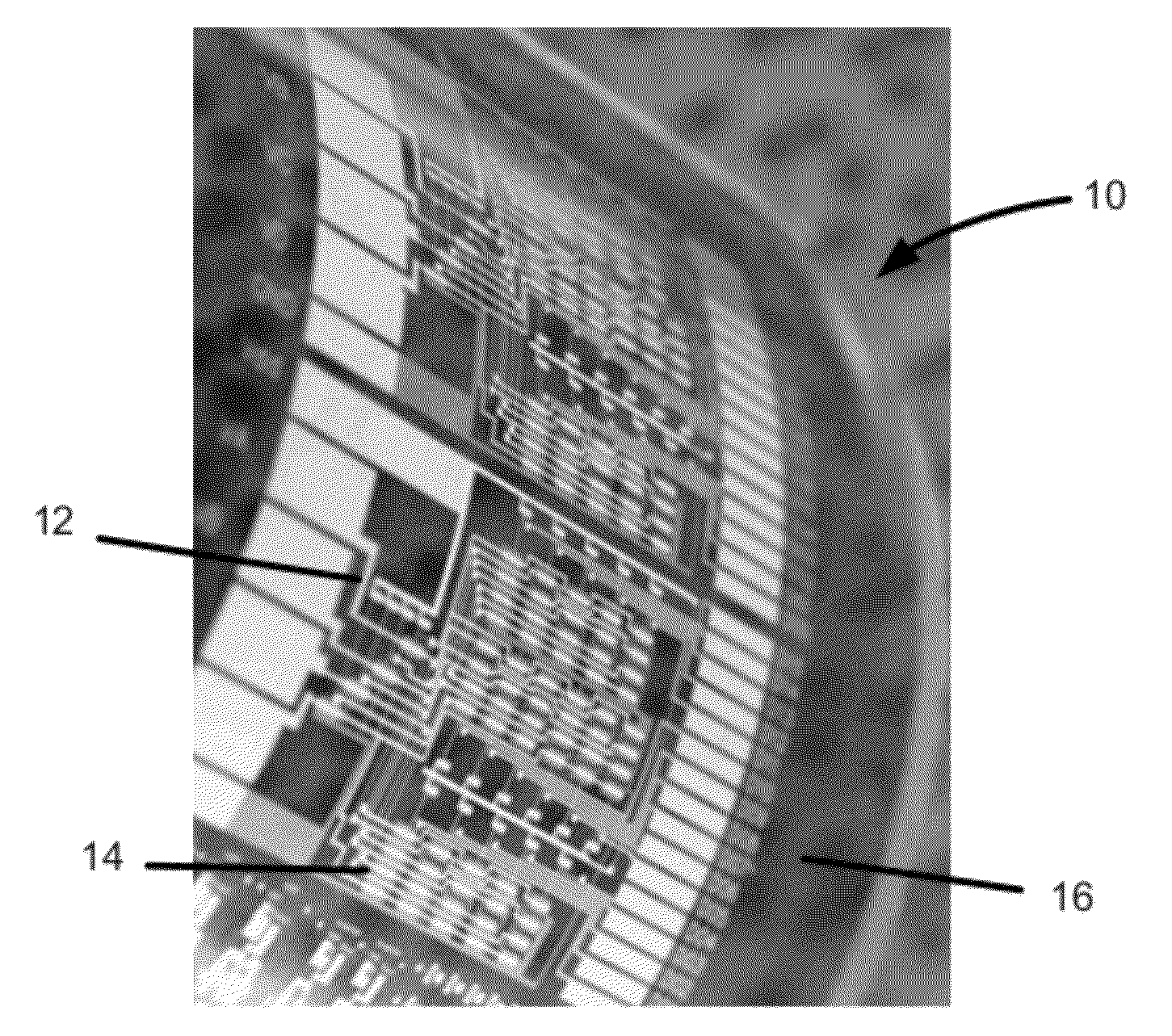
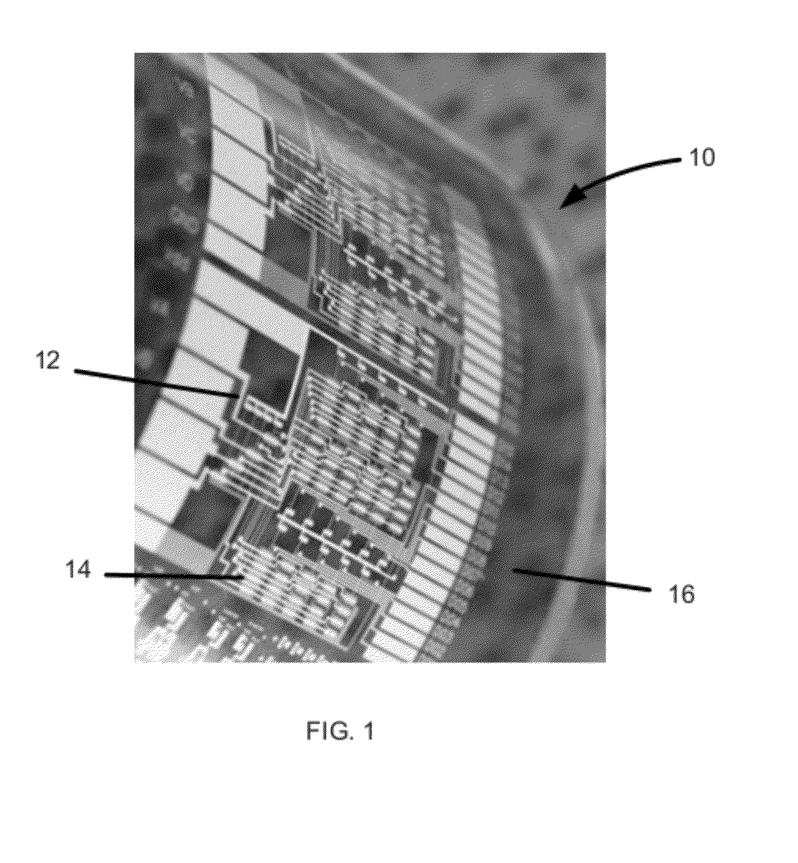
[0010]The present invention includes the printing of electronic circuits and elements using copper nanoparticles, which enables the creation of copper circuits and elements onto a variety of rigid and flexible substrates at pitches below 100 micrometers. When nanoparticles having a diameter of under 20 nanometers, preferably under 10 nanometers, more preferably in the range of 1-7 nanometers, and even more preferably in the range of 3-5 nanometers, are printed onto a substrate in a manner similar to that of inkjet printers, the nanoparticles fuse upon impact with the substrate. Copper nanoparticles of these sizes can also be applied in a pattern and fused by exposure to a short-duration pulse of radiant energy, such as a laser or a bright light, or by exposure to a temperature of less than 200° C., and preferably less than 70° C. Copper nanoparticles of these sizes can also be fused by pressure such as compression under a form or by tracing the desired pattern with a mechanical stylus such as a nanoinscriber. Forming circuit elements in the methods described herein allows the use of substrate materials, and particularly flexible materials, that cannot tolerate the chemicals and temperatures of the current processes used to create circuit elements on substrates for electronic assemblies. The methods of printing and forming circuit elements from copper nanoparticles as described herein also enable finer pitch circuits, i.e. having small separation distances between conductive elements, than possible with other processes. Circuit elements formed from copper nanoparticles may include passive devices such as resistors, capacitors, and inductors, active devices such as transistors, Radio Frequency (RF) elements such as antennae, reflectors, and waveguides, other circuit elements such as ground and power planes, shielding, and signal paths, and even complete devices such as a Radio Frequency IDentification (RFID) tag.
[0011]In certain embodiments, a circuit element is disclosed that comprises a first layer of formed metal comprising fused nanoparticles that comprise copper and had a diameter of less than 20 nanometers prior to being fused.
[0012]In certain embodiments, a circuit assembly is disclosed that comprises a substrate and a first layer of formed metal coupled to the substrate, the first layer of formed metal comprising fused nanoparticles that comprise copper and had a diameter of less than 20 nanometers prior to being fused.
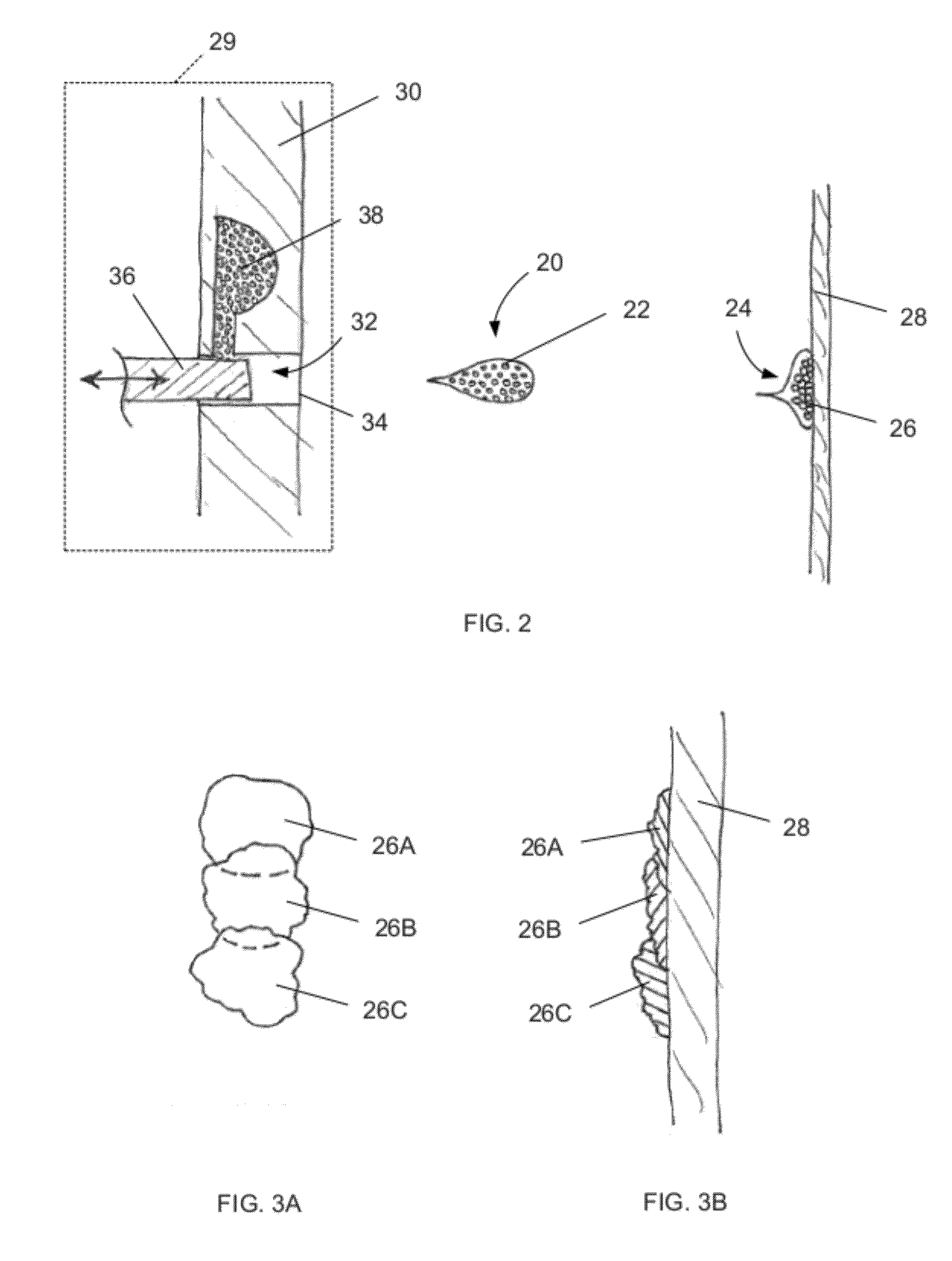
[0013]In certain embodiments, a circuit-printing device is disclosed that comprises a sprayer configured to emit a plurality of drops of a mixture comprising nanoparticles that comprise copper and have a diameter of less than 20 nanometers toward a substrate with sufficient velocity that the nanoparticles fuse with each other upon impact with the substrate and form a plurality of dots on the substrate, wherein each dot comprises a layer of fused nanoparticles and overlapping dots are fused to each other.
[0014]In certain embodiments, a method of creating a conductive element on a substrate is disclosed. The method comprising the step of spraying a plurality of drops of a mixture comprising nanoparticles that comprise copper and have a diameter of less than 20 nanometers toward a substrate with sufficient velocity that the nanoparticles fuse with each other upon impact with the substrate and form a plurality of dots on the substrate, wherein each dot comprises a layer of fused nanoparticles and overlapping dots are fused to each other.
[0015]In certain embodiments, a method of creating a conductive element on a substrate is disclosed. The method comprising the steps of applying a layer of a mixture comprising nanoparticles that comprise copper and have a diameter of less than 20 nanometers over at least a portion of a surface of a substrate, and fusing the nanoparticles together in at least a portion of the mixture layer.

Problems solved by technology

The minimum separation of the traces is often limited by the etching process.
Each of the processes have advantages and disadvantages related to resolution, throughput, and cost.

Method used


Image

  • Copper nanoparticle application processes for low temperature printable, flexible/conformal electronics and antennas
  • Copper nanoparticle application processes for low temperature printable, flexible/conformal electronics and antennas
  • Copper nanoparticle application processes for low temperature printable, flexible/conformal electronics and antennas

Examples


Embodiment Construction

[0031]Some inkjet printers use a piezoelectric actuator to eject a drop of ink from an ink-filled chamber or channel beneath each nozzle. When a voltage is applied, the piezoelectric material changes shape, creating a pressure wave in the channel that ejects a droplet of ink from the nozzle with sufficient velocity to reach the paper on which the image is being created. Piezoelectric inkjet technology allows the use of a wider variety of inks than thermal inkjet technology as there is no requirement for a volatile component, and no issue with kogation of the ink. One printing process is referred to as “drop-on-demand”, wherein software directs the printheads to eject one or more droplets of ink from a nozzle only when it is desired to create an image on the portion of the paper immediately in front of the nozzle.

[0032]Copper particles having diameters of less than 20 nanometers have properties that are not linear extensions of their bulk properties. At these diameters, copper nanopa...


PUM

PropertyMeasurementUnit
diameteraaaaaaaaaa
diameteraaaaaaaaaa
diameteraaaaaaaaaa

Abstract

An ink adapted for forming conductive elements is disclosed. The ink includes a plurality of nanoparticles and a carrier. The nanoparticles comprise copper and have a diameter of less than 20 nanometers. Each nanoparticle has at least a partial coating of a surfactant configured to separate adjacent nanoparticles. Methods of creating circuit elements from copper-containing nanoparticles by spraying, tracing, stamping, burnishing, or heating are disclosed.

Description

CROSS-REFERENCES TO RELATED APPLICATIONS[0001]The present application is related to U.S. application Ser. No. 12 / 512,315, filed Jul. 30, 2009 and currently pending.Statement Regarding Federally Sponsored Research or Development[0002]Not Applicable.BACKGROUND[0003]1. Field[0004]The present invention relates to printed electronics and, in particular, the creation of circuit elements using copper nanoparticles.[0005]2. Description of the Related Art[0006]Electrical assemblies are currently fabricated using a rigid substrate with individual components attached to the substrate and interconnected with conductive paths or “traces” on the substrate. The traces are typically created on the surface of the substrate by coating the entire surface of the substrate with a layer of copper, masking the copper with the interconnect pattern using a photolithographic process, and selectively etching away the non-masked copper. The minimum separation of the traces is often limited by the etching proce...

Claims


Application Information

Patent Timeline
Patent Type & Authority Applications(United States)
IPC IPC(8): H05K1/00B05C5/00B05D5/12B05D3/12B05D3/06H01B1/02H05K3/14B82Y99/00C01B32/50
CPCH01L27/124H01L21/4867C09D11/322C09D11/52H05K3/02H05K3/4069H05K2203/0108H05K2203/0126H05K2203/0143H05K2203/0278H05K2203/107H05K1/097H05K3/1283H05K2203/1131H01L27/1292H05K1/028H05K3/14
Inventor ZINN, ALFRED A.
Owner KUPRION INC
Why Eureka
Try Eureka