

Group iii nitride semiconductor light-emitting device
a technology of nitride and semiconductor light, which is applied in the direction of semiconductor devices, semiconductor lasers, semiconductor lasers, etc., can solve the problems that the group iii nitride semiconductor light-emitting device having excellent characteristics is difficult to fabricate, and achieves good morphology, excellent characteristics, and uniform physical properties.
- Summary
- Abstract
- Description
- Claims
- Application Information
AI Technical Summary
Benefits of technology
Problems solved by technology
Method used
Image

Examples
example a
1. Preparation of GaN Crystal Substrate
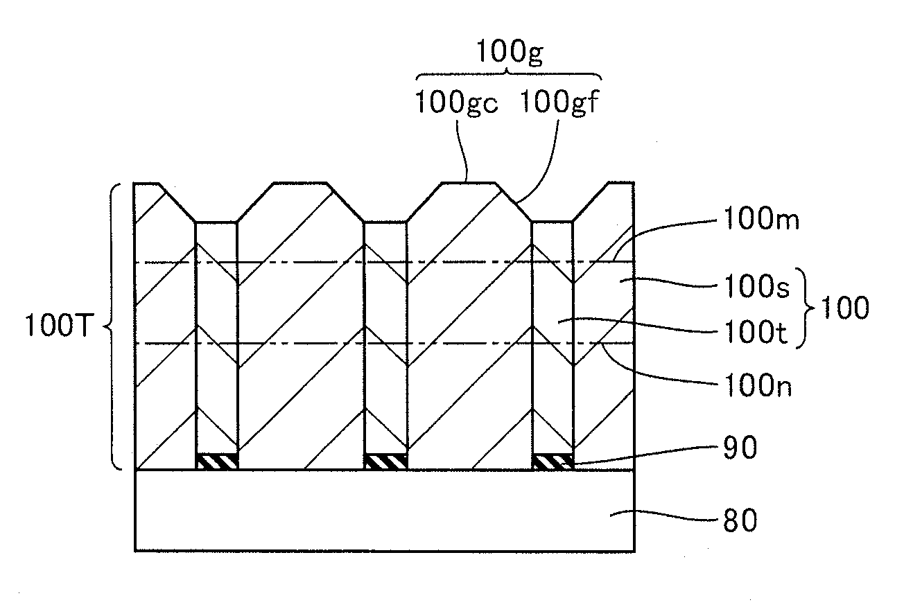
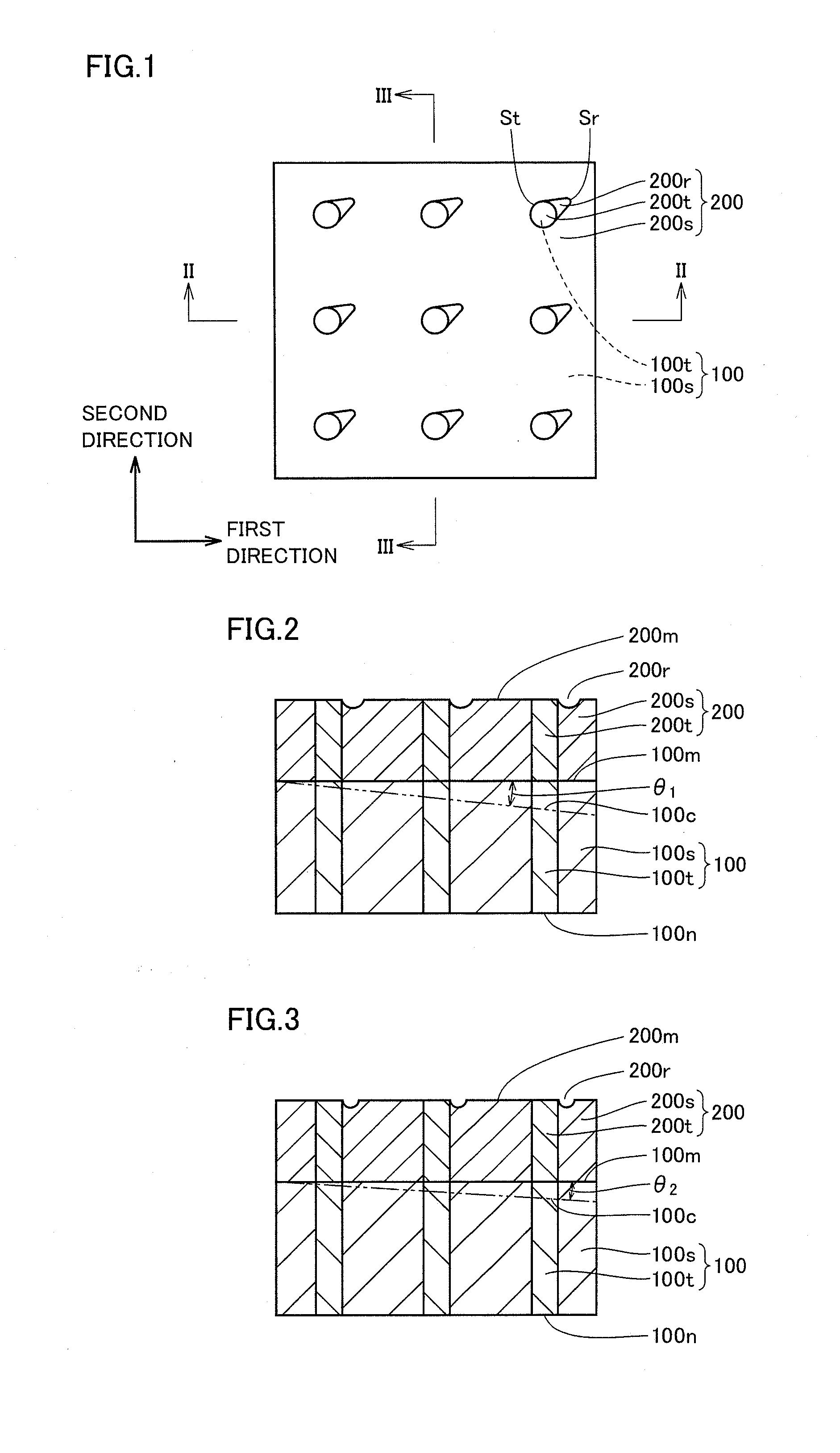
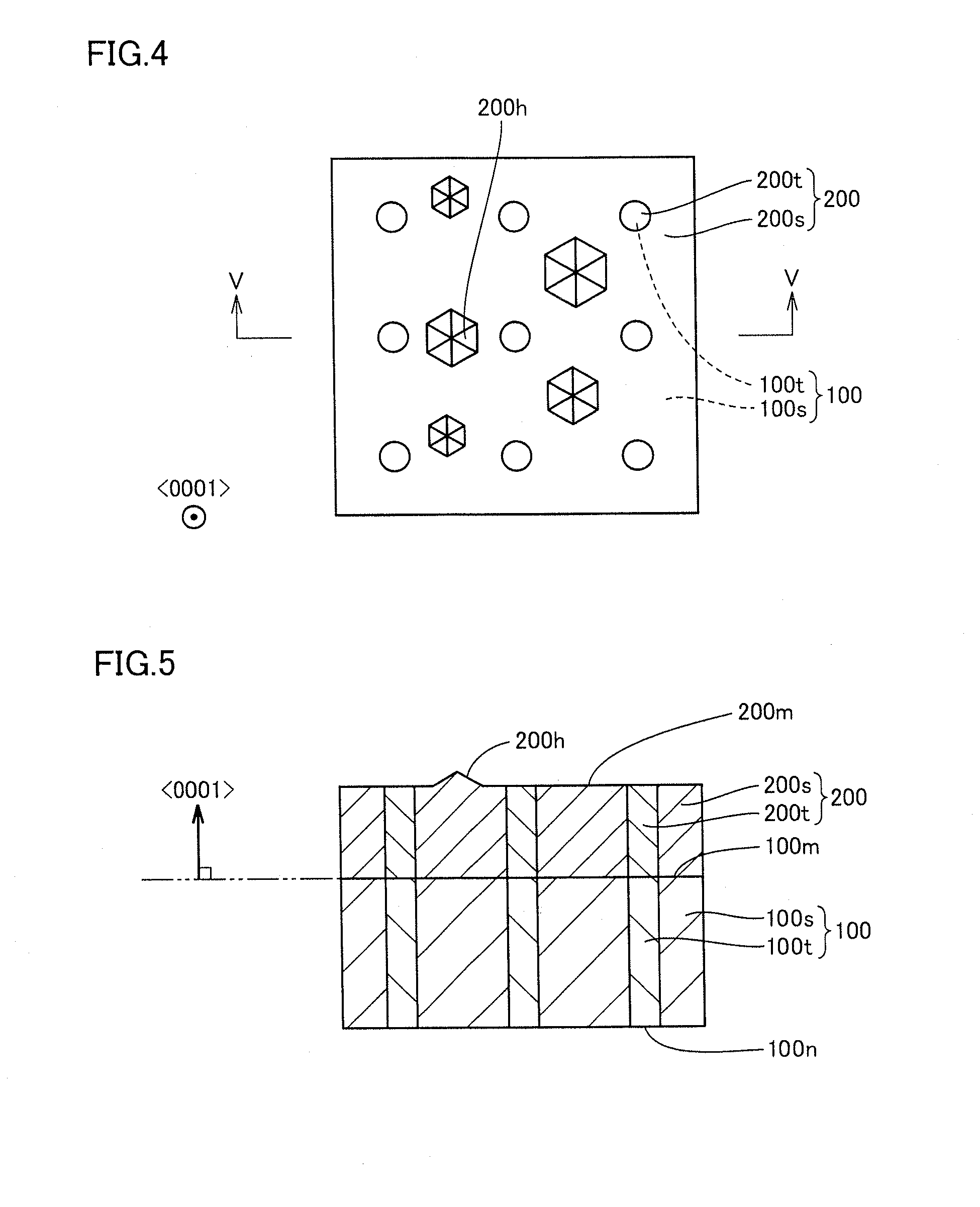
[0090]GaN crystal substrates of 17 different types having a diameter of two inches (5.08 cm) and a thickness of 400 μm were prepared (Examples AR-1 to AR-3 and Examples A-1 to A-14). The GaN crystal substrates each included a matrix crystal region and a c-axis-inverted crystal region. On the front main surface of the substrate, the c-axis-inverted crystal region was arranged in the form of dots on square lattice points. The dots had a diameter of 60 μm and the pitch between the dots was 1000 μm. The front main surface had a predetermined off angle θ with respect to the {0001} plane, and the front main surface and the rear main surface had a predetermined warp. In Example A, the direction was defined as the first direction of off angle θ and the direction was defined as the second direction of off angle θ.
[0091]Here, regarding off angle θ between the front main surface of the GaN crystal substrate and the {0001} plane, absolute value |θ1| of t...
example b
[0109]1. Preparation of GaN Crystal Substrate
[0110]GaN crystal substrates of 17 different types were prepared in a similar manner to Example A, except that the direction was defined as the first direction of off angle θ and the direction was defined as the second direction of off angle θ.
[0111]Regarding each of the GaN crystal substrates of 17 different types, absolute value |θ2| of the off-angle component of the direction, absolute value |θ1| of the off-angle component of the direction, the warp of the front main surface, and the warp of the rear main surface were as follows. Regarding the GaN crystal substrate of Example BR-1, they were 0.95°, 0.99°, 11.9 μm, and 11.9 μm, respectively. Regarding the GaN crystal substrate of Example BR-2, they were 0.59°, 0.66°, −9.6 μm, and 4.5 μm, respectively. Regarding the GaN crystal substrate of Example BR-3, they were 0.10°, 0.09°, 7.8 μm, and 4.5 μm, respectively. Regarding the GaN crystal substrate of Example B-1, they were 0.78°, 1.08...
example c
[0119]I. Preparation of GaN Crystal Substrate
[0120]GaN crystal substrates of 11 different types were prepared in a similar manner to Example A.
[0121]Regarding each of the GaN crystal substrates of the 11 different types, absolute value |θ1| of the off-angle component of the direction, absolute value |θ2| of the off-angle component of the direction, the warp of the front main surface, and the warp of the rear main surface were as follows. Regarding the GaN crystal substrate of Example CR-1, they were 1.09°, 0.93°, 8.9 μm, and 12.0 μm, respectively. Regarding the GaN crystal substrate of Example CR-2, they were 0.65°, 0.65°, −7.8 μm, and −5.7 μm, respectively. Regarding the GaN crystal substrate of Example CR-3, they were 0.10°, 0.11°, 8.9 μm, and −11.2 μm, respectively. Regarding the GaN crystal substrate of Example C-1, they were 1.06°, 0.77°, −14.3 μm, and 12.8 respectively. Regarding the GaN crystal substrate of Example C-2, they were 0.03°, 0.02°, 4.5 μm, and −11.5 μm, respecti...
PUM
 Abstract
Description
Claims
Application Information