Vialess memory structure and method of manufacturing same

a memory structure and memory technology, applied in the field of semiconductor memory, can solve the problems of undefeated connection between the mtj and the upper metal line, limited process margin for etching, and difficult manufacturing of the mram

Active Publication Date: 2012-12-06
AVALANCHE TECH
View PDF13 Cites 13 Cited by
  • Summary
  • Abstract
  • Description
  • Claims
  • Application Information

AI Technical Summary

Problems solved by technology

Manufacturing of the MRAM has offered challenges.
Conversely, the shallow via hole often makes no contact with the top electrode because during the via etching process, the bottom of the via does not reach the top electrode of the MTJ resulting in an undesirably open connection between the MTJ and the upper metal line.
The process margin for etching is therefore limited.
Efforts have been used to overcome this problem by using a thick top electrode formed on top of the MTJ but this presents a challenge for fine patterning including photo and etch processes.
Thick photo resist and / or thick hard mask is required to make a pattern in the top electrode, which does not meet the requirements for fine patterning since fine patterning requires thin photoresist and hard mask.
Further, there are multiple steps employed in building an MTJ with a separate step needed for making the via, which adds to manufacturing time and expense.

Method used


Image

  • Vialess memory structure and method of manufacturing same
  • Vialess memory structure and method of manufacturing same
  • Vialess memory structure and method of manufacturing same

Examples


Embodiment Construction

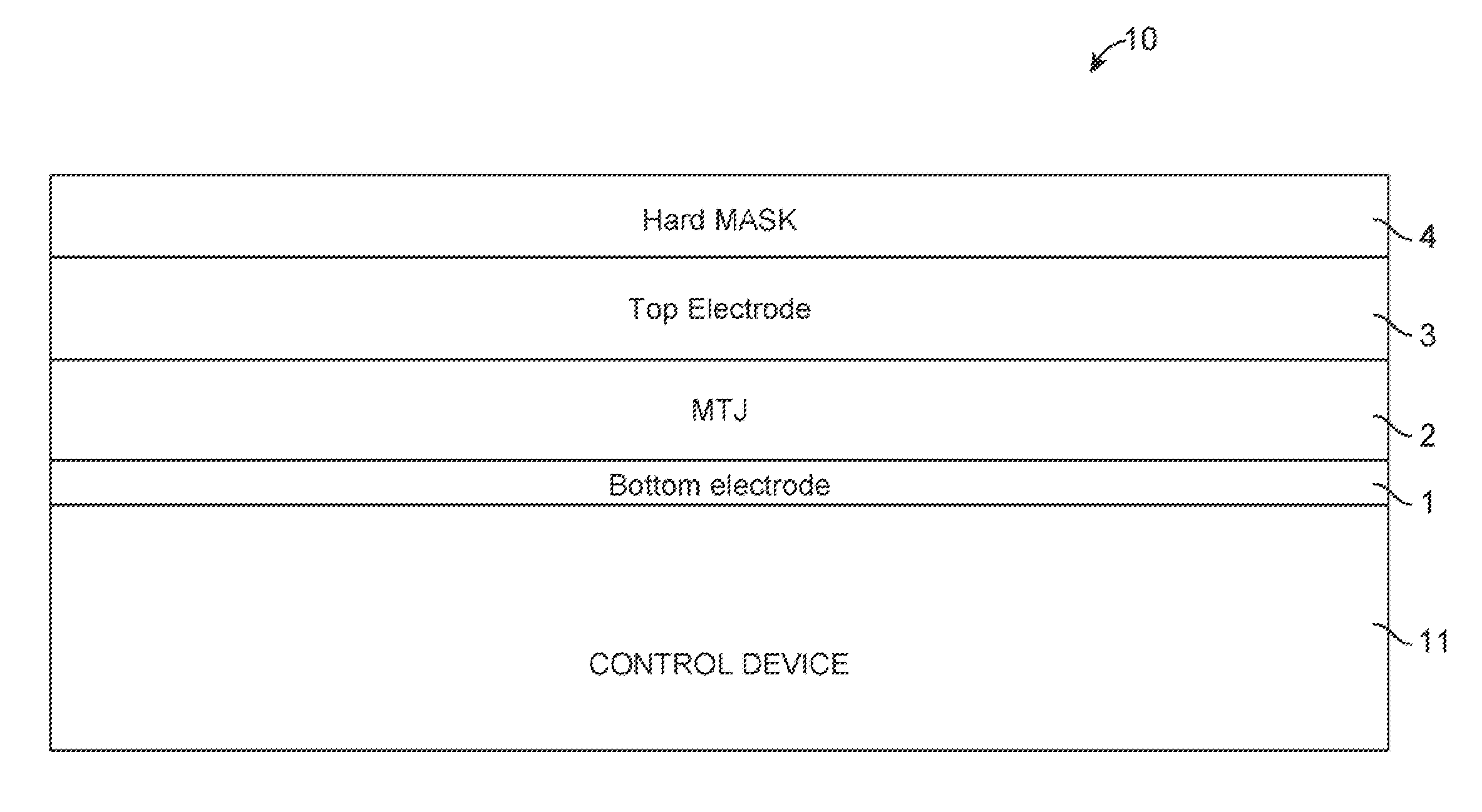
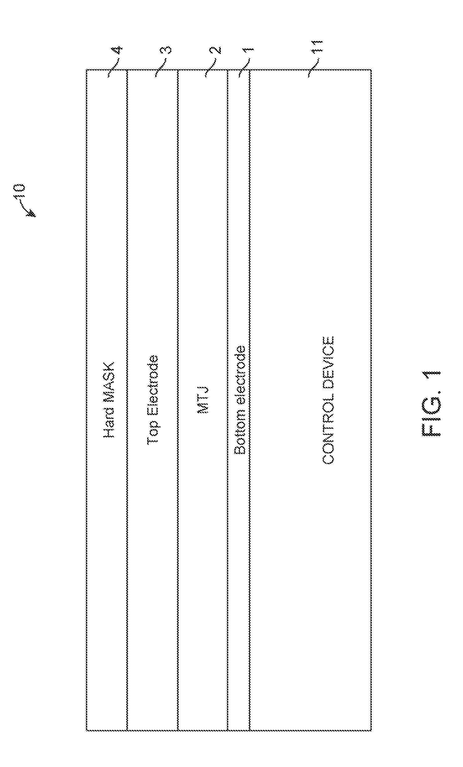
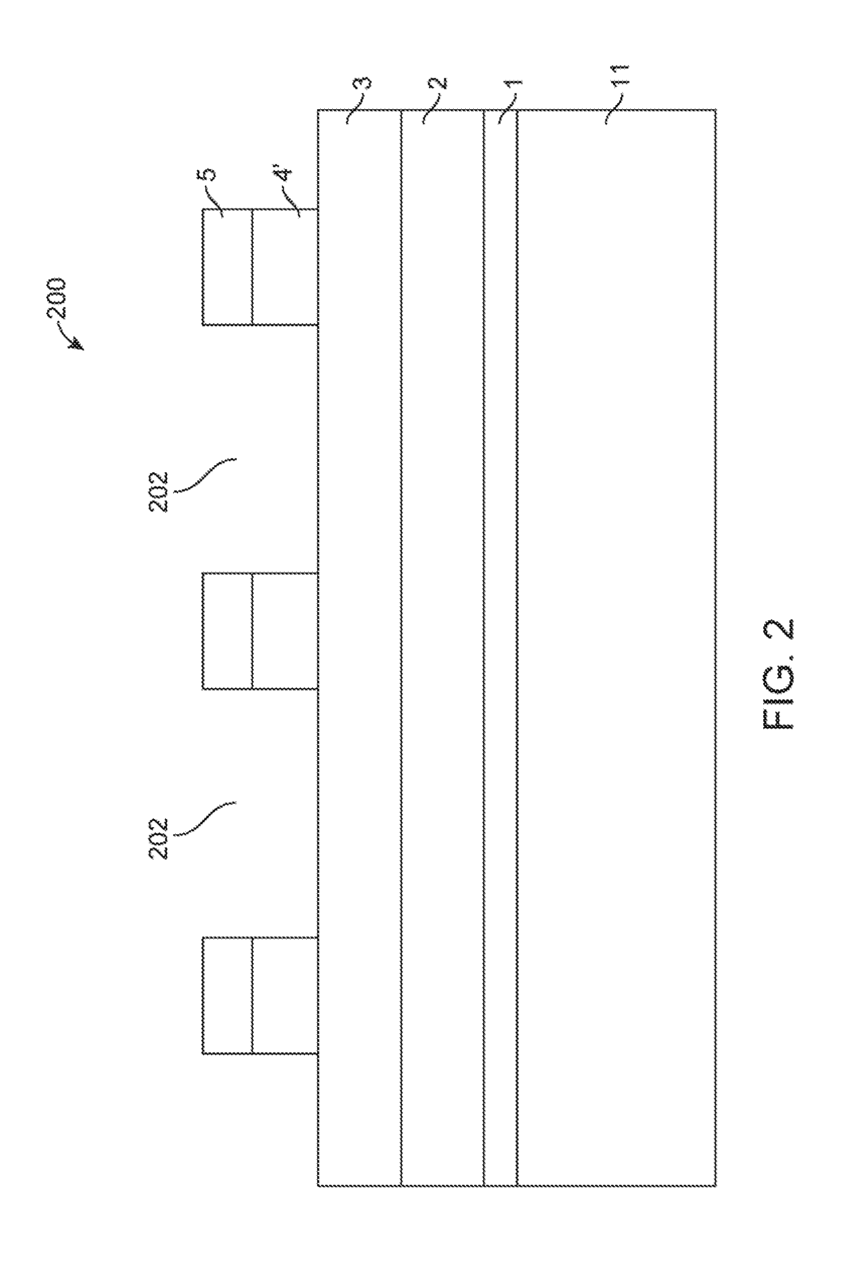
[0014]In the following description of the embodiments, reference is made to the accompanying drawings that form a part hereof, and in which is shown by way of illustration of the specific embodiments in which the invention may be practiced. It is to be understood that other embodiments may be utilized because structural changes may be made without departing from the scope of the present invention. It should be noted that the figures discussed herein are not drawn to scale and thicknesses of lines are not indicative of actual sizes.

[0015]In an embodiment and method of the present invention, methods of fabricating magnetic memory cell are disclosed. A magneto (or “magnetic”) tunnel junction (MTJ) is included in the magnetic memory cell and a metal line is directly connected to the MTJ without the need for a via. As will be disclosed, various methods of manufacturing a magnetic memory cell, which includes a magnetic tunnel junction (MTJ), are disclosed to protect the MTJ sidewall with ...


PUM

PropertyMeasurementUnit
sizeaaaaaaaaaa
thicknessaaaaaaaaaa
thickaaaaaaaaaa

Abstract

A method of manufacturing a magnetic memory cell, including a magnetic tunnel junction (MTJ), includes using silicon nitride layer and silicon oxide layer to form a trench for depositing copper to be employed for connecting the MTJ to other circuitry without the use of a via.

Description

BACKGROUND OF THE INVENTION[0001]1. Field of the Invention[0002]The present invention relates generally to semiconductor memory and method of manufacturing the same and particularly to via-less memory structures and method of manufacturing same.[0003]2. Description of the Prior Art[0004]Magnetic random access memory (MRAM) is rapidly gaining popularity as its use in replacing conventional memory is showing promise. MRAM memory element consists of a top electrode connecting to a bit line, a magnetic tunnel junction (MTJ), and a bottom electrode connecting to a control device such as a FET transistor or a diode. The MTJ further includes a free layer, a pinned layer and a barrier layer. Manufacturing of the MRAM has offered challenges.[0005]The size of the memory element has been reduced to minimize the memory cell area. It has become smaller than the size of the via, the latter being used to form a connection to the MTJ and to an upper metal line serving as a bit line. A side wall of ...

Claims


Application Information

Patent Timeline
Patent Type & Authority Applications(United States)
IPC IPC(8): H01L43/02H01L43/12
CPCH01L43/12H01L27/222H10B61/00H10N50/01H10B61/10H10B61/22H10N50/10
Inventor SATOH, KIMIHIROHUAI, YIMINGZHANG, JING
Owner AVALANCHE TECH
Why Eureka
Try Eureka