Manufacturing method for thin film semiconductor device, manufacturing method for thin film semiconductor array substrate, method of forming crystalline silicon thin film, and apparatus for forming crystalline silicon thin film

a manufacturing method and semiconductor technology, applied in the field of manufacturing methods for thin film semiconductor array substrates, can solve the problems of large input energy and laser facilities for higher output, complex laser facilities, etc., and achieve the effect of improving the turn-on characteristics of the thin film semiconductor device and increasing the crystal grain size of the crystalline silicon thin film without increasing the laser output energy

Inactive Publication Date: 2012-12-06
JOLED INC
View PDF14 Cites 7 Cited by
  • Summary
  • Abstract
  • Description
  • Claims
  • Application Information

AI Technical Summary

Benefits of technology

[0017]According to the manufacturing method for the thin film semiconductor device according to the present invention, it is possible to increase the crystal grain size of the crystalline silicon t

Problems solved by technology

However, if the maximum intensity of the laser beam is simply increased, this necessitates the laser beam with larger output energy.
As a result, there are problems that larger input energy and laser facility for higher output are necessary.
In this case, laser irradiation f

Method used


Image

  • Manufacturing method for thin film semiconductor device, manufacturing method for thin film semiconductor array substrate, method of forming crystalline silicon thin film, and apparatus for forming crystalline silicon thin film
  • Manufacturing method for thin film semiconductor device, manufacturing method for thin film semiconductor array substrate, method of forming crystalline silicon thin film, and apparatus for forming crystalline silicon thin film
  • Manufacturing method for thin film semiconductor device, manufacturing method for thin film semiconductor array substrate, method of forming crystalline silicon thin film, and apparatus for forming crystalline silicon thin film

Examples


embodiment

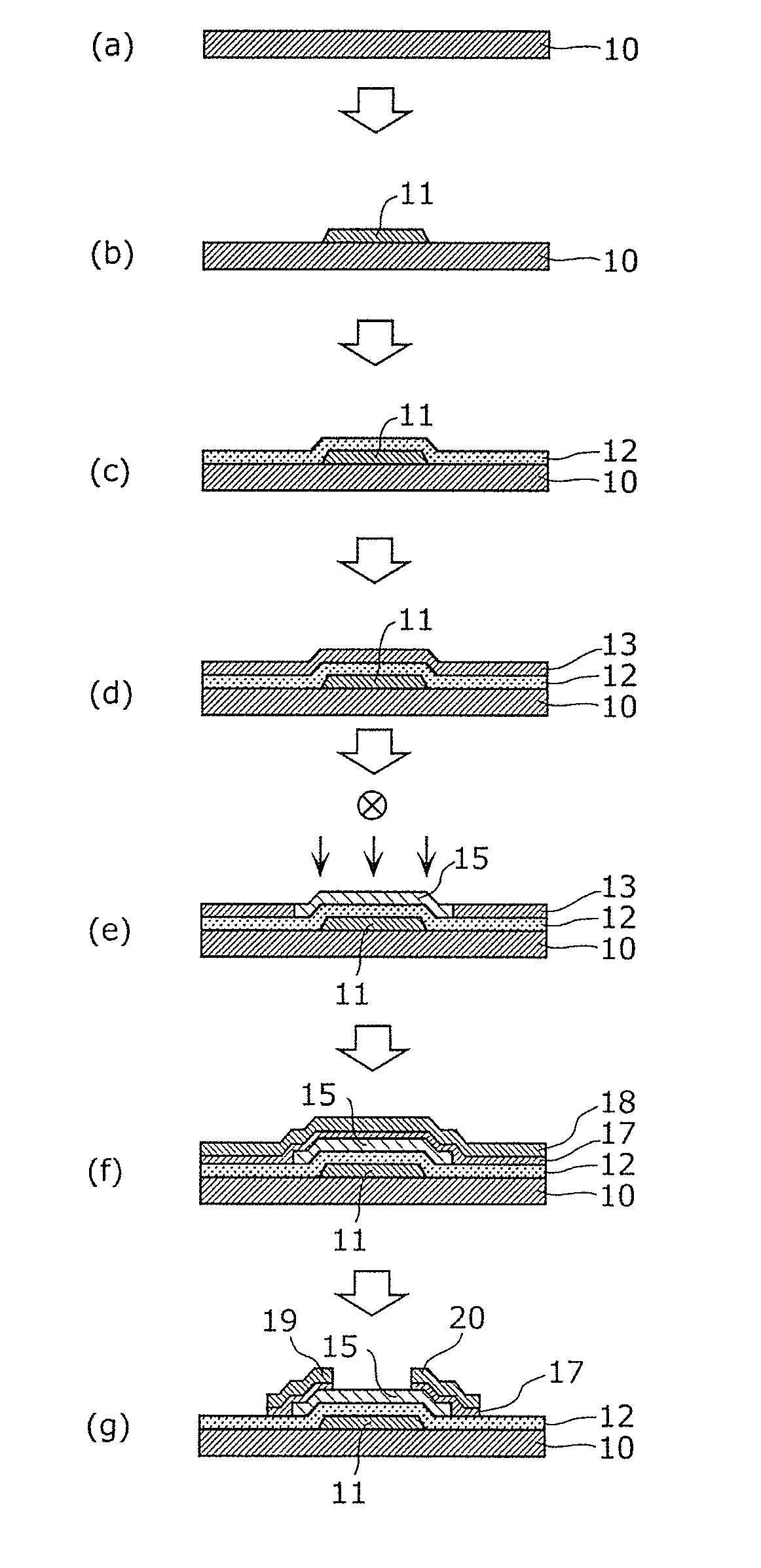
[0065]The following shall describe a manufacturing method for a thin film semiconductor device, a manufacturing method for a thin film semiconductor array substrate, a method of forming a crystalline silicon thin film, and an apparatus for forming the crystalline silicon thin film according to the present invention, with reference to the drawings.

(Method of Forming Crystalline Silicon Thin Film)

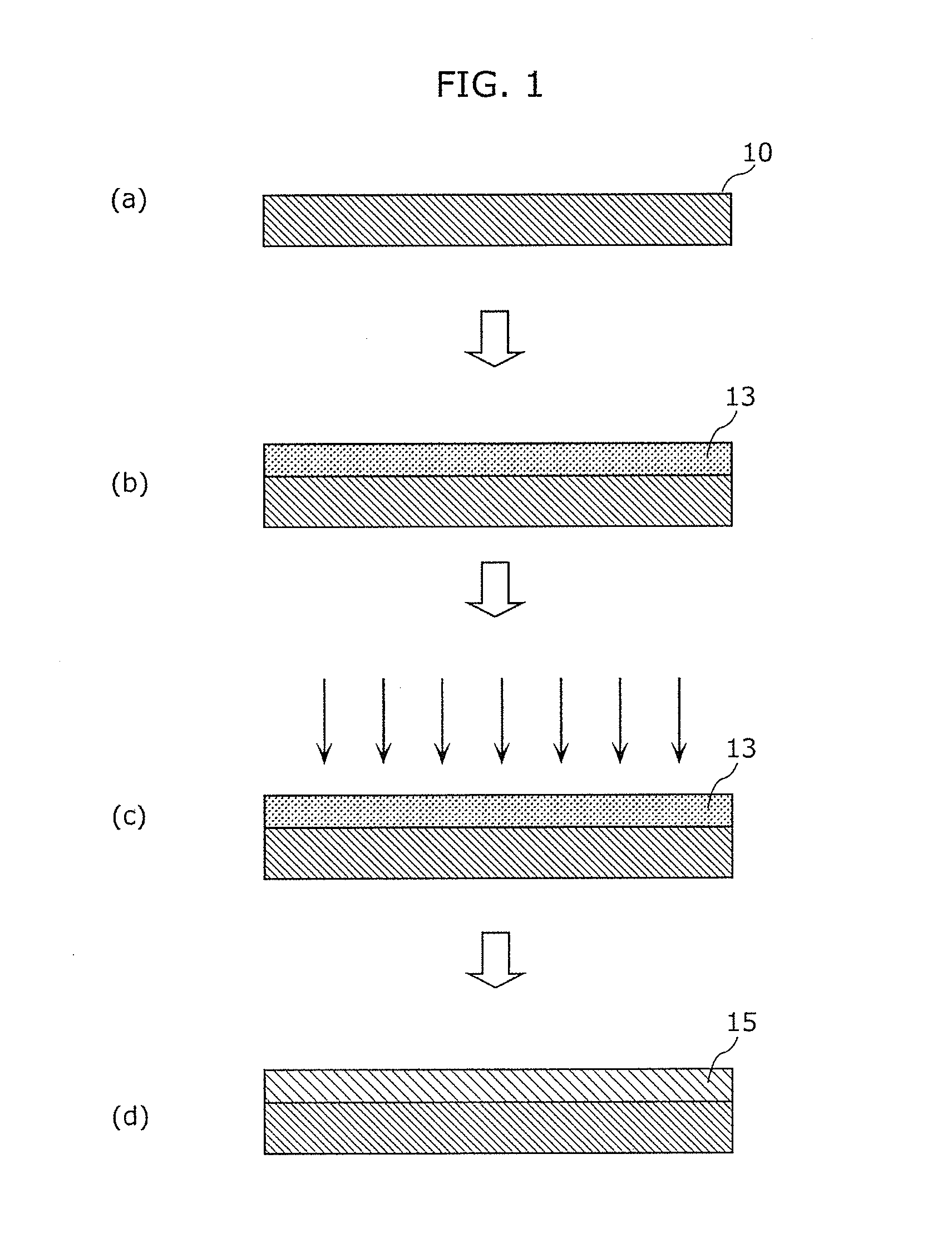
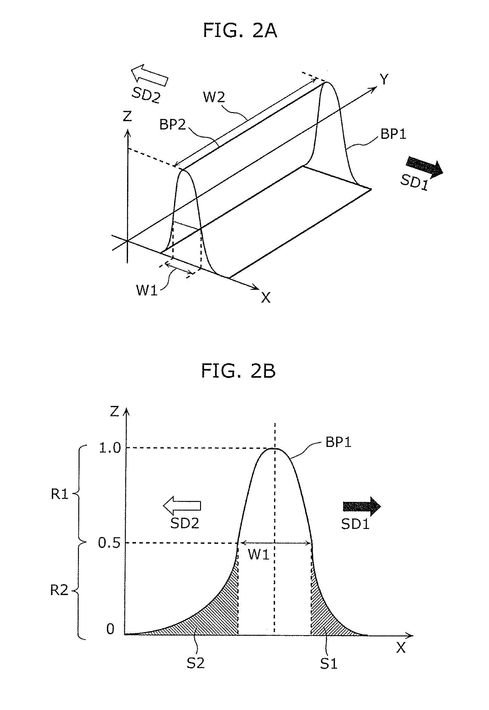
[0066]First, a method of forming a crystalline silicon thin film according to the embodiment of the present invention shall be described with reference to FIGS. 1, 2A, and 2B. FIG. 1 includes cross-sectional views of processes in the method of forming the crystalline silicon thin film according to the embodiment of the present invention. FIG. 2A illustrates an intensity distribution (beam profile) of CW laser beam used in a silicon thin film crystallizing process in the method of forming the crystalline silicon thin film according to the present invention. FIG. 2B illustrates an intensity dis...


PUM


Abstract

A crystalline silicon thin film is formed by irradiating a silicon thin film with a laser beam. The laser beam is a continuous wave laser beam. An intensity distribution of the laser beam in a first region about a center of the intensity distribution is symmetric on an anterior side and a posterior side of the center. The intensity distribution in a second region about the center is asymmetric on the anterior side and the posterior side. The first region is from the maximum intensity of the laser beam at the center to an intensity half of the maximum intensity. The second region is at most equal to the half of the maximum intensity of the laser beam. In the second region, an integral intensity value on the posterior side is larger than on the anterior side.

Description

CROSS REFERENCE TO RELATED APPLICATION[0001]This is a continuation application of PCT Patent Application No. PCT / JP2011 / 003109, filed on Jun. 2, 2011, designating the United States of America, the disclosure of which, including the specification, drawings and claims, is incorporated herein by reference in its entirety.BACKGROUND OF THE INVENTION[0002]1. Field of the Invention[0003]The present invention relates to a manufacturing method for thin film semiconductor device, a manufacturing method for a thin film semiconductor array substrate, a method of forming a crystalline silicon thin film, and an apparatus for forming a crystalline silicon thin film.[0004]2. Description of the Related Art[0005]In an active-matrix driven display device such as an organic electro luminescence (EL) display apparatus or a liquid crystal display, thin film semiconductor devices known as thin film transistors (TFT) are used.[0006]In this type of display apparatus, an array of the thin film transistors c...

Claims


Application Information

Patent Timeline
IPC IPC(8): H01L21/336B01J19/12H01L21/20
CPCH01L21/02532H01L21/02678H01L27/1285H01L21/02691H01L29/66765H01L21/02683H01L21/18H01L21/20H01L21/786
Inventor ODA, TOMOHIKOKAWASHIMA, TAKAHIRO
Owner JOLED INC
Why Eureka
Try Eureka