Method of fabricating semiconductor devices

a technology of semiconductor devices and semiconductor layers, applied in the direction of semiconductor devices, basic electric elements, electrical equipment, etc., can solve the problems of difficult epitaxial growth of sige, conventional method of forming -shaped sige, and difficulty in the epitaxial growth of seed layers

Active Publication Date: 2012-12-06
SEMICONDUCTOR MANUFACTURING INTERNATIONAL (BEIJING) CORP
View PDF13 Cites 15 Cited by
  • Summary
  • Abstract
  • Description
  • Claims
  • Application Information

AI Technical Summary

Benefits of technology

[0013]According to another specific embodiment, the step of changing the characteristic includes performing an oxidation process on the substrate. According to another specific embodiment, the oxidation process includes a wet oxidation process. According to another specific embodiment, the step of performing an orientation selective wet etching process on the recess includes using tetramethylammonium hydroxide (TMAH). According to another specific embodiment, the etching rate of the orientation selective wet etching on a (100) crystal orientation plane is faster than that on a (111) crystal orientation plane. According to another specific embodiment, the orientation selective wet etching substantially stops on the (111) crystal orientation of plane. According to another specific embodiment, the first material is polysilicon.
[0015]According to another specific embodiment, the method of fabricating a semiconductor device further includes, before changing the characteristic of a portion of the substrate process, forming a mask overlaying an area to be formed as a NMOS device and exposing an area to be formed as a PMOS device. According to another specific embodiment, the second material is silicon nitride. According to another specific embodiment, the etching rate of the orientation selective wet etching on a (100) crystal orientation plane is faster than that on a (111) crystal orientation plane.

Problems solved by technology

However, conventional method of forming Σ-shaped SiGe suffer from the problem of difficult SiGe epitaxial growth.
Defects such as Si lattice mismatch can lead to the difficulty in the epitaxial growth of a seed layer.
Hence, as shown in FIG. 1E, Si lattice defects at points C and D will make the subsequent defect free epitaxial growth of a SiGe seed layer difficult to achieve.

Method used


Image

  • Method of fabricating semiconductor devices
  • Method of fabricating semiconductor devices
  • Method of fabricating semiconductor devices

Examples


Embodiment Construction

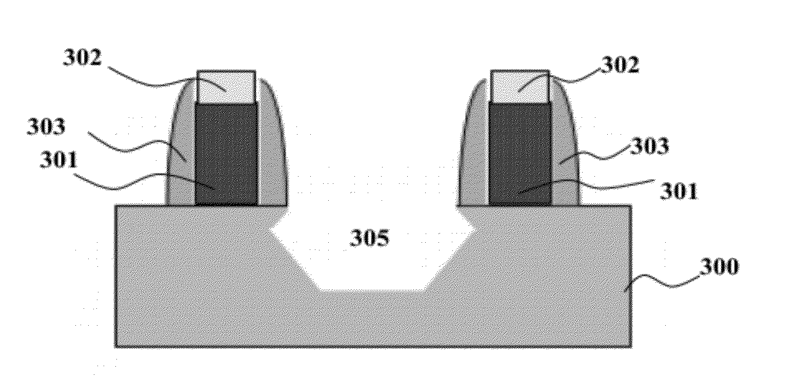
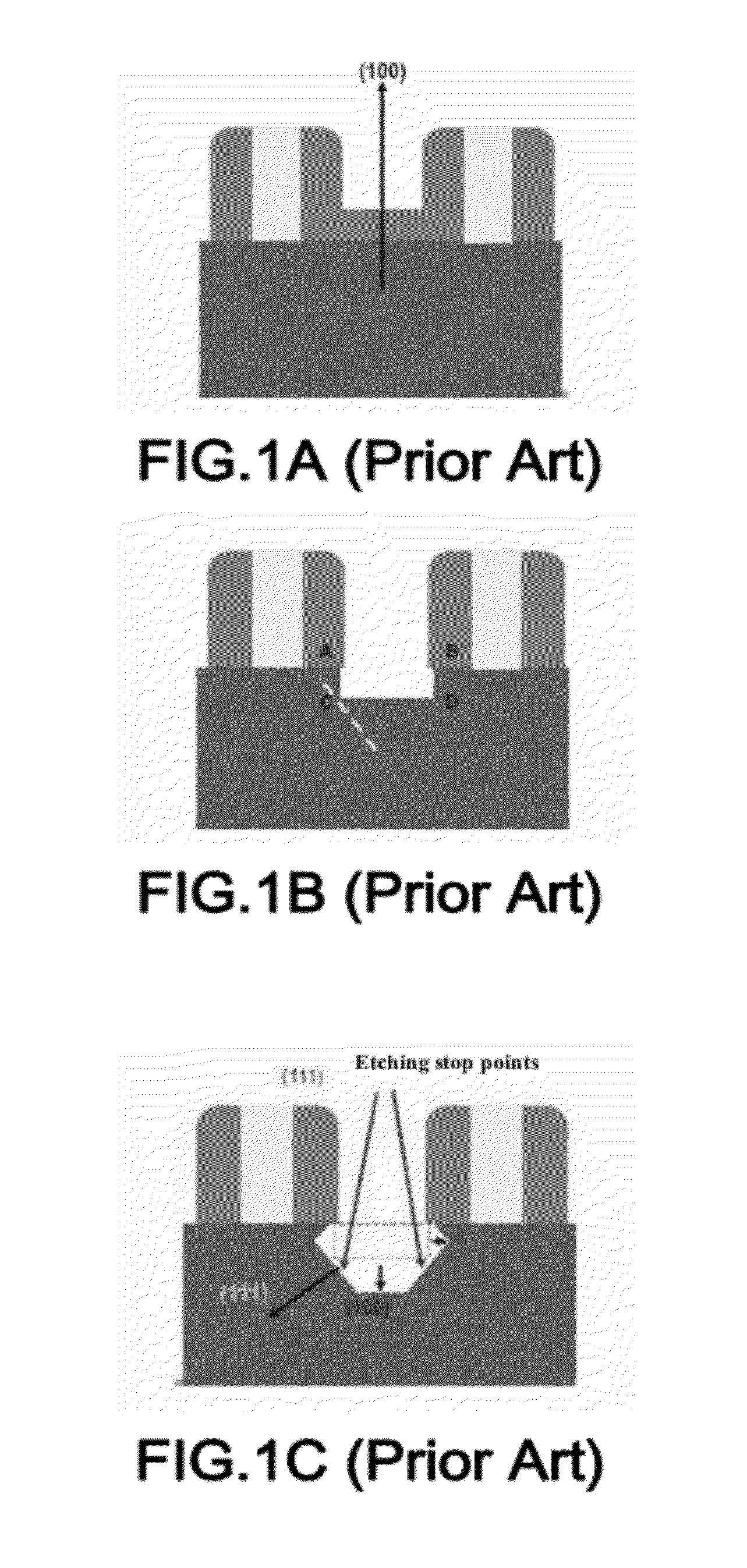
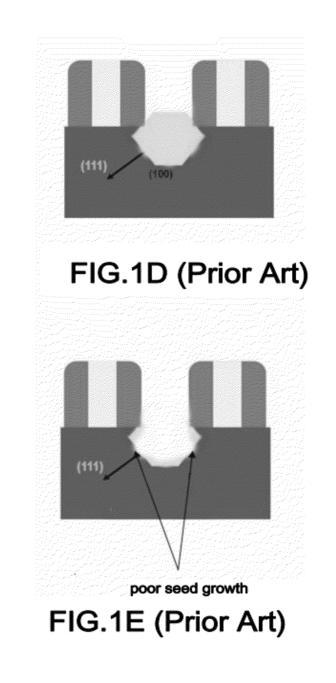
[0025]According to embodiments of the present invention, a method for fabricating semiconductor devices including PMOS devices having embedded SiGe (eSiGe) is provided. In an embodiment of this disclosure, instead of using dry etching which may damage the lattice structure of the substrate, first, a characteristic of predetermined portion of the substrate is changed by a process such as ion implantation or oxidation; next, the substrate portion with the changed characteristic is removed by isotropic wet etching to form a substantially rectangular recess in the substrate; then, the inner walls of the recess are shaped into sigma-shape (Σ-shape) by orientation selective wet etching. The sigma-shaped recess is then epitaxially filled in with SiGe. Thus, the substrate is prevented from being damaged and adverse effects on the subsequent epitaxial growth of SiGe are avoided.

[0026]FIG. 2 schematically shows a flowchart of a method of forming a Σ-shaped recess in a PMOS device, in accordan...


PUM


Abstract

A method of fabricating a semiconductor device is provided. The method includes forming a gate having a first material on a substrate and a layer of a second material overlaying the gate. Sidewall spacers are formed on opposite sides of the gate. A characteristic of a portion of the substrate between adjacent sidewall spacers is changed using the layer of second material and the sidewall spacers as a mask. An isotropic wet etch process is performed to remove the substrate portion with a changed characteristic to form a recess in the substrate. An orientation selective wet etching process is performed on the recess to shape the inner walls of the recess into sigma-shape. Changing a substrate characteristic in conjunction with isotropic wet etching prevents the substrate from being damaged, and therefore can obtain defect free epitaxial SiGe growth performance.

Description

CROSS-REFERENCES TO RELATED APPLICATIONS[0001]This application claims priority to Chinese Patent Application No. 201110147173.2, filed on Jun. 2, 2011 and entitled “Method of Fabricating Semiconductor Devices”, which is incorporated herein by reference in its entirety. This application is related to commonly assigned U.S. patent application Ser. No. ______, filed Nov. 9, 2011, having Attorney Docket No. 87720-821445 (027900US), and commonly assigned U.S. patent application Ser. No. ______, filed Nov. 9, 2011, having Attorney Docket No. 87720-821441 (028000US), the contents of all of which are incorporated herein by reference in their entirety.BACKGROUND[0002]1. Field of the Invention[0003]The present disclosure relates to a method of fabricating semiconductor devices, and particularly to a method of fabricating semiconductor devices including PMOS devices having embedded SiGe (eSiGe).[0004]2. Description of the Related Art[0005]In order to meet the demand of users for low profile el...

Claims


Application Information

Patent Timeline
Patent Type & Authority Applications(United States)
IPC IPC(8): H01L21/336
CPCH01L21/26506H01L21/823412H01L21/823425H01L21/823807H01L21/823814H01L29/165H01L21/3086H01L29/66636H01L29/78H01L29/7848H01L21/30604H01L21/30608H01L29/66575H01L21/26566
Inventor ZHANG, YIYINGHE, QIYANG
Owner SEMICONDUCTOR MANUFACTURING INTERNATIONAL (BEIJING) CORP
Why Eureka
Try Eureka