Fin-Last Replacement Metal Gate FinFET

a technology of fin-last and gate, which is applied in the field of integrated circuits, can solve the problems of difficult alignment of landing pads with gate, significant fabrication challenges, and inability to properly and consistently contact source and drain

Inactive Publication Date: 2012-12-13
AURIGA INNOVATIONS INC
View PDF8 Cites 152 Cited by
  • Summary
  • Abstract
  • Description
  • Claims
  • Application Information

AI Technical Summary

Benefits of technology

[0010]The present invention provides improved fin field effect transistor (FinFET) devices and methods for the fabrication thereof. In one aspect of the invention, a method for fabricating a field effect transistor device is provided. The method includes the following steps. A wafer is provided having an active layer on an insulator. A plurality of fin hardmasks are patterned on the active layer. A dummy gate is placed over a central portion of the fin hardmasks, wherein portions of the active layer outside of the dummy gate will serve as source and drain regions of the device. One or more doping agents are implanted into the source and drain regions. A dielectric filler layer is deposited around the dummy gate. The dummy gate is removed to form a trench in the dielectric filler layer, wherein the fin hardmasks are present on the active layer in the trench. The fin hardmasks are used to etch a plurality of fins in the active layer within the trench, wherein the fins will serve as a channel region of the device. The doping agents implanted into the source and drain regions are activated using rapid thermal annealing. A replacement gate is formed in the trench, wherein the step of activating the doping agents implanted into the source and drain regions is performed before the step of forming the replacement gate in the trench.

Problems solved by technology

The architecture of a FinFET device, however, presents notable fabrication challenges.
For example, as feature sizes of the devices get increasingly smaller (commensurate with current technology) accurately and consistently contacting the source and drain becomes a problem.
Properly and consistently aligning the landing pads with the gate is difficult.
Without landing pads however, contact has to be made with individual fins, which can be difficult, e.g., due to mismatches between minimum fin pitch and minimum pitch for contact vias.
Epitaxial processes, however, have drawbacks due to their extreme sensitivity to surface chemistry, crystal orientation and growth conditions.
Scaling fin width is another challenge for FinFET manufacturing.
For schemes where the fins are formed before gate patterning, thin fins must survive gate and spacer processing, which often involves aggressive etching processes.
The teachings of Schulz, however, do not provide for formation of fins with the precision and consistency needed for manufacture, especially in the context of scaled process technology.

Method used


Image

  • Fin-Last Replacement Metal Gate FinFET
  • Fin-Last Replacement Metal Gate FinFET
  • Fin-Last Replacement Metal Gate FinFET

Examples


Embodiment Construction

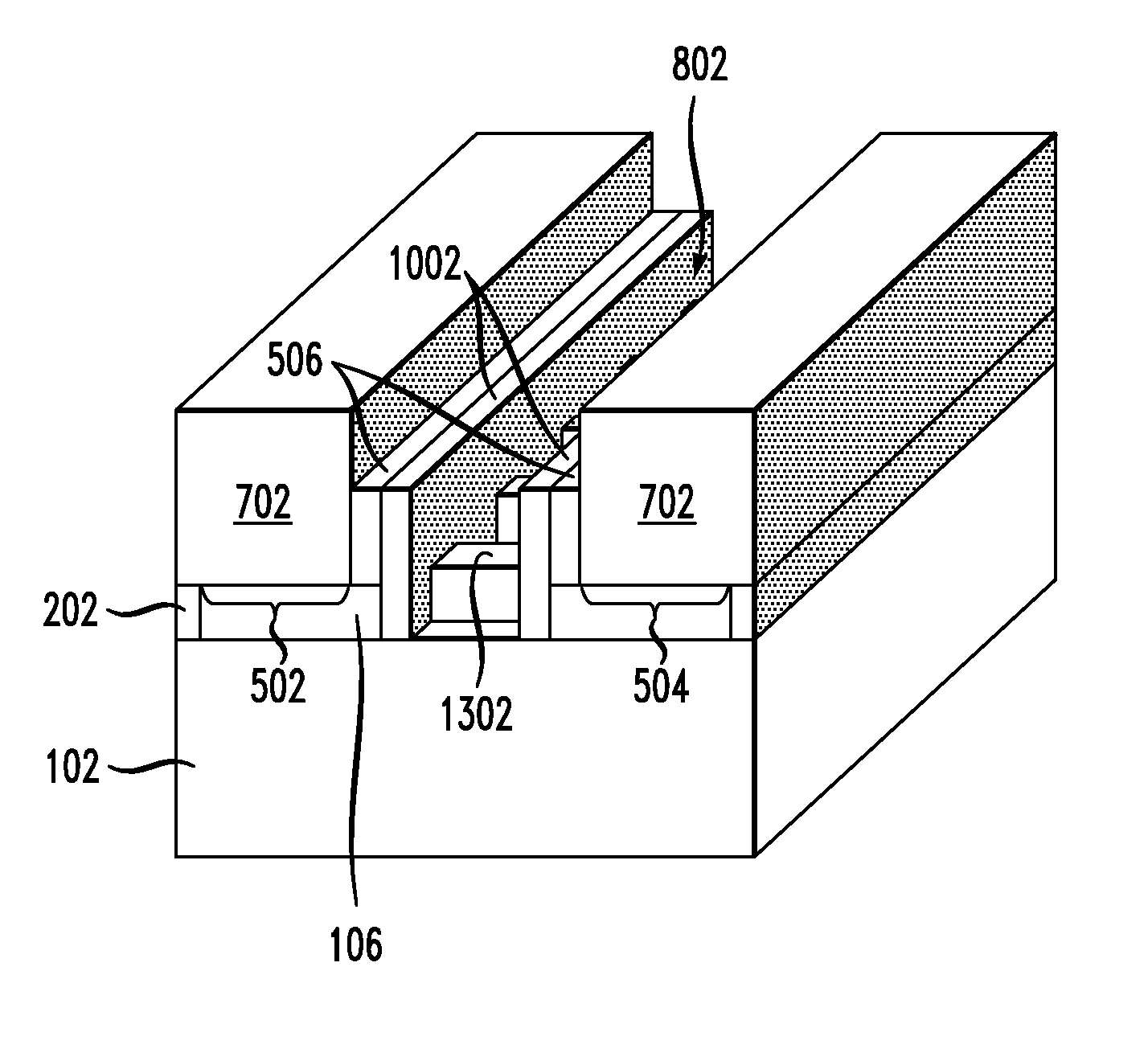
[0042]FIGS. 1-15 are diagrams illustrating an exemplary methodology for fabricating a fin field effect transistor (FinFET) device. As will be described in detail below, the present techniques make use of a damascene gate process to construct source / drain regions that are self-aligned with the gate.

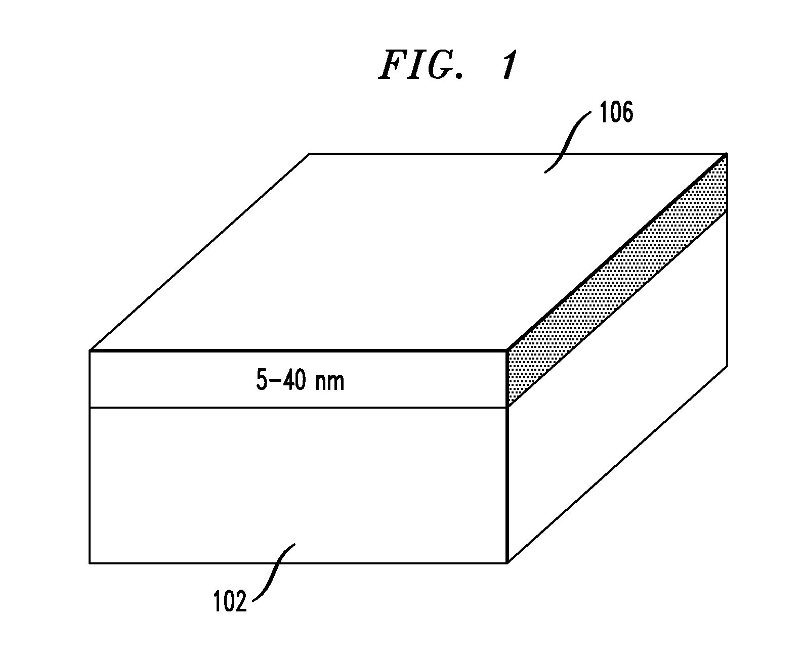
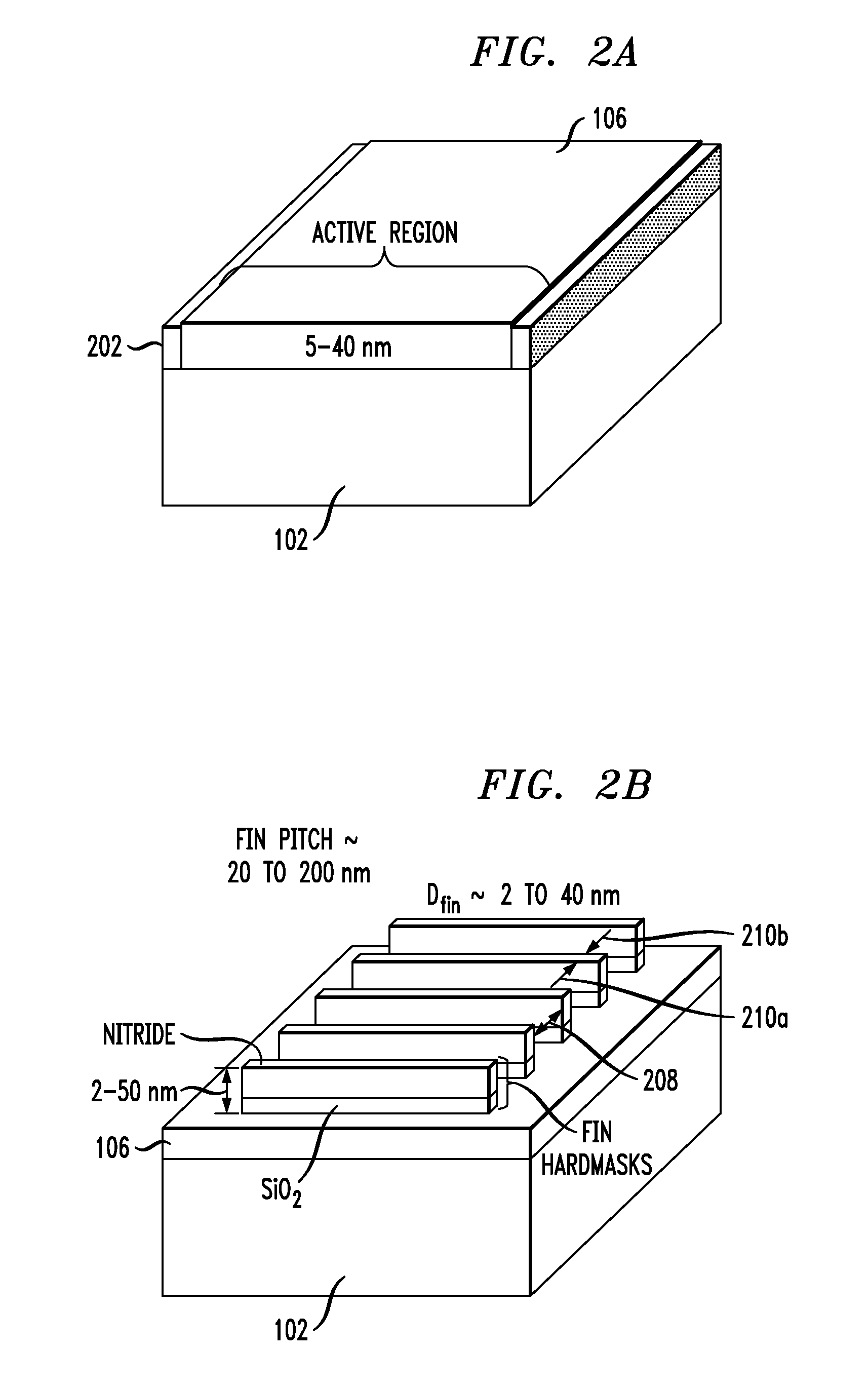
[0043]The fabrication process begins with a semiconductor-on-insulator (SOI) wafer. See FIG. 1. An SOI wafer typically includes a layer of a semiconductor material (also commonly referred to as a semiconductor-on-insulator layer or SOI layer) separated from a substrate by an insulator. When the insulator is an oxide (e.g., silicon dioxide (SiO2)), it is commonly referred to as a buried oxide, or BOX. According to the present techniques, the SOI layer will serve as an active layer of the device. Thus, the SOI layer will be referred to herein as an active layer. In the example shown in FIG. 1, the starting wafer includes an active layer 106 over a BOX 102. For ease of depiction, a substrate ...


PUM


Abstract

FinFET devices and methods for the fabrication thereof are provided. In one aspect, a method for fabricating a FET device includes the following steps. A wafer is provided having an active layer on an insulator. A plurality of fin hardmasks are patterned on the active layer. A dummy gate is placed over a central portion of the fin hardmasks. One or more doping agents are implanted into source and drain regions of the device. A dielectric filler layer is deposited around the dummy gate. The dummy gate is removed to form a trench in the dielectric filler layer. The fin hardmasks are used to etch a plurality of fins in the active layer within the trench. The doping agents are activated. A replacement gate is formed in the trench, wherein the step of activating the doping agents is performed before the step of forming the replacement gate.

Description

FIELD OF THE INVENTION[0001]The present invention relates to integrated circuits, and more particularly, to fin field effect transistor (FinFET) devices and methods for fabrication thereofBACKGROUND OF THE INVENTION[0002]Due to their fast switching times and high current densities, fin field effect transistor (FinFET) devices are of a desired device architecture. In its basic form, a FinFET device includes a source, a drain and one or more fin-shaped channels between the source and the drain. A gate electrode over the fin(s) regulates electron flow between the source and the drain.[0003]The architecture of a FinFET device, however, presents notable fabrication challenges. For example, as feature sizes of the devices get increasingly smaller (commensurate with current technology) accurately and consistently contacting the source and drain becomes a problem. Some previous demonstrations of FinFET devices have been on single fins, isolated devices or devices built at a greatly relaxed ...

Claims


Application Information

Patent Timeline
Patent Type & Authority Applications(United States)
IPC IPC(8): H01L21/336H01L29/78B82Y40/00B82Y99/00
CPCH01L29/66545H01L29/785H01L29/1037H01L29/66795
Inventor CHANG, JOSEPHINE B.GUILLOM, MICHAEL A.HAENSCH, WILFRIED ERNST-AUGUST
Owner AURIGA INNOVATIONS INC
Why Eureka
Try Eureka